| John Broskie's Guide to Tube Circuit Analysis & Design |
16 December 2023 Post Number 575
Cascoding Chip Amplifiers
In this circuit, all the NPN transistors (Q1, Q3, Q5) experience the same emitter-to-collector voltage swings, while each only contributes one third of the output current swings; as a result, they will all dissipate the same amount of heat. (The same applies to all the PNP transistors.) As long as the output stage remains within its window of class-A operation, the output impedance will roughly equal the resistance of one emitter resistor divided by six. Once the output current swing exceeds the class-A limit, the output impedance will increase by twofold. (Of course, this is based on no negative feedback having been applied.) The cascode configuration, in contrast, places the output devices in series, so that all the NPN transistors experience the same output current swings, but only a portion of the output voltage swings.
In this schematic, all four output transistors share the same emitter-to-collector voltage, but we could alter the ratio from the 50% shown here, perhaps giving the top and bottom transistors a greater slice of the voltage. Unlike the parallel arrangement, the cascode does not lower the output impedance nor increase the maximum current delivery over a single pair of output devices. So why cascode? Long ago, say before the mid-1970s, the only way we could make high-power transistor-based power amplifiers was to use cascoded output transistors, as the maximum emitter-to-collector voltage was only a fraction of what is available today. With the development of power transistors capable of withstanding up to 260V, the practice of cascading fell out of favor. Nonetheless, the cascoding of output devices offers some real advantages. For example, with a 50% split, we halve the Miler-effect capacitance and quarter that of two in parallel. In addition, we can use dissimilar technologies; for instance, we can use expensive lateral MOSFETs in the center position and cheap VMOS, HEXFET, MDmesh™, PowerTrench… in the outside positions. Why? We can get the features of both types of MOSFET, i.e. the negative tempco of the L-MOSFET and easy biasing, along with the high-power and low-cost of the VMOS MOSFET. Indeed, we can mix bipolar transistors and MOSFETs, with the transistors in the center position, cascoded by MOSFETs. This arrangement works well, as it is relatively easy to the drive the MOSFETs, but not the transistors.
Note that the voltage division is not 50-50 in this example. Why not? High-wattage MOSFET are relatively cheap, so we can burden them with more of the voltage and heat dissipation. This brings us to the topic of cascoding a chip amplifier. Why would we want to do so? The obvious answer is more power output. The less obvious answer is better heat dissipation.
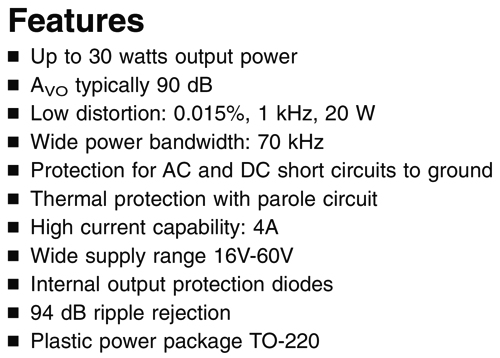
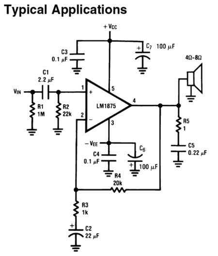
Here is an example: the LM1875 has a small following who love the sound from the TO-220-packaged IC power amplifier, but the tiny amplifier is a hassle to implement. The data sheet details its features:
If we read the LM1875 data sheet (always a good idea), we see the following:
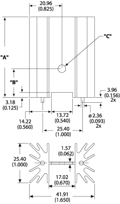
Okay we must always use a heatsink, but how big should it be? Big, really big. The data sheet recommends a heatsink with a thermal resistance of 0.6°C/W, which implies big, heavy, and expensive. We can forget about using PCB-mount heatsinks, such as the Aavid Thermalloy 530002B02500G heatsink, a 2.5-inch tall heatsink with a thermal resistance of 2.6°C/W.
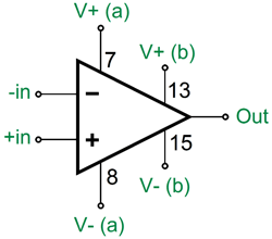
This heatsink would be good for only about 10W to 12W of dissipation with the LM1875, which would translate into only about 8W of signal output. A trick often used with the LM1875, however, is to use it with a monopolar power supply, as the LM1875's tab is connected to its negative power-supply pin, which means ground potential with a single power-supply voltage. In other words, we do not need to isolate the tab of the heatsink, although we should use some thermal grease. Indeed, often the metal casework is the heatsink with IC power amplifiers like the LM1875. On the other hand, if we add two cascode output devices, we can offload much of the heat dissipation to them. Well, how hard would it be to build a cascoded power amplifier with a chip amplifier? The answer is it depends. If we are using a TDA7293 chip amplifier, it is no big deal, as the TDA7293 offers us two sets of positive and negative power-supply pins, one set for both the input stage and driver stage and one set for just the output stage.
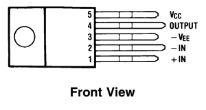
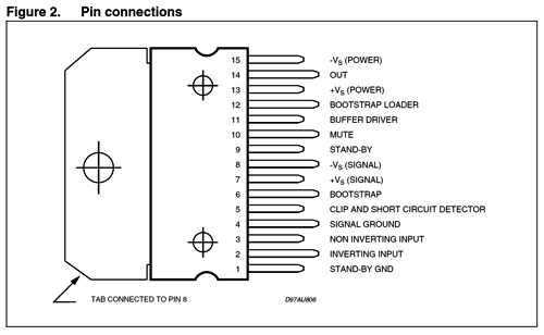
This is a wonderful feature, which I wish National Semi had followed in designing their chip amplifiers; for example, the LM1875 could have been housed in the 7-pin TO-220 package instead of the 5-pin version. Here is the pin out for the TDA7293.
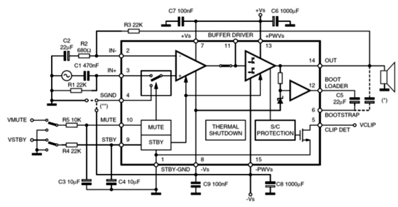
And here it is in use:
If your brain melted after looking at the schematic, just ignore it and look at the following schematic of a simple solid-state power amplifier with two sets of power-supply connections.
The two sets of V+ and V- connections can be bridged or attached to dissimilar voltages. Indeed, many advantages accure from giving the input and VAS stages their own higher voltage power-supply voltages than the output stage. (Often in existing power amplifiers, we see RC filters separating the raw bipolar power-supply voltages from the input and VAS stages. By removing the RC resistors, we can implement the two sets of power-supply connections.) Perhaps, I have gone too far, so I will retreat to baby steps. Let's ignore what exactly is inside the power amplifier and look at how we can add cascoding to only its output devices.
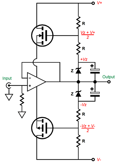
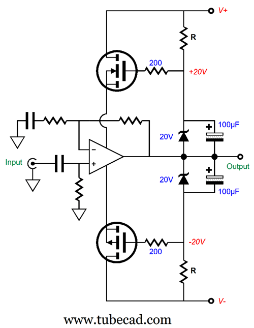
Here we see the output stage getting the cascode treatment, while the input stage and driver stage share the connections to the full positive and negative power-supply rail voltages. With the 20V zener diodes, the output stage will see bipolar power supply voltage of about +/-15Vdc, thereby greatly limiting the output stage's dissipation, as the top and bottom MOSFETs share the heat burden. For example, if the bipolar power-supply rail voltages are +/-60Vdc, each MOSFET will see a 45V voltage drop at idle. A better arrangement is the following, which uses a lower-valued zener voltage and two-resistor voltage dividers to create a setup wherein the output stage sees half of the bipolar power supply voltages and we run less of a risk of damaging the MOSFETs due to excessive gate-to-source voltages when the amplifier delivers full output.
Before going any further with cascoded power amplifiers, we should examine the simpler arrangement of cascoding a power buffer—if for no other reason that buffers are conceptually simpler than amplifiers.
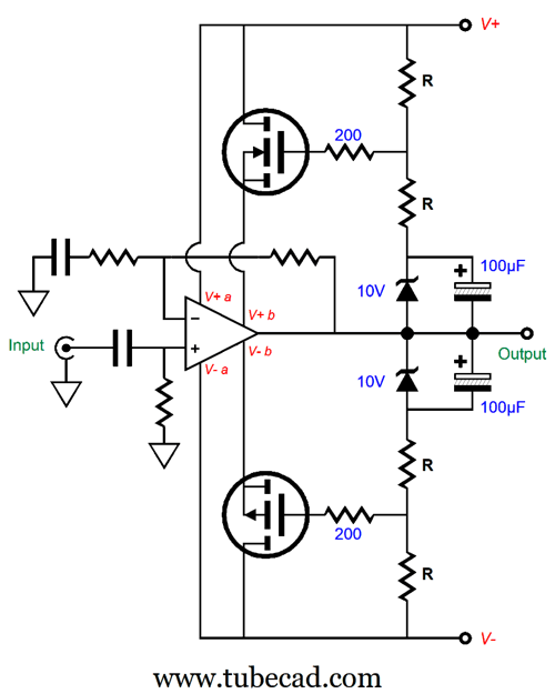
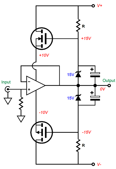
Cascoded Power Buffers
The two 15V zener diodes establish the +15V and -15V gate voltages for the top and bottom power MOSFETs. Since the MOSFETs are "enhancement" types, the gate voltage must be greater relative to the source voltage. With most power MOSFET this turn-on falls between 4V to 5V, which explains why the power buffer's power-supply rail voltages are +/-10Vdc in this example. The bipolar power supply voltage is not marked, but it could be as low as +/-20Vdc to +/-200Vdc. The voltage limit is set by the P-MOSFET, as the highest-voltage P-MOSFET I know of is the IXTH20P50P, with a source-to-drain voltage limit of -500V. For audio use, such as driving loudspeakers, a more reasonable power-supply rail voltages of +/-30Vdc to +/-60Vdc would be expected. With +/-40Vdc bipolar power-supply rail voltages, the buffer sees 25% of the differential power-supply voltage, so it will dissipate only 25% of the heat at idle, with the two MOSFETs equally sharing the remaining 75% of the heat dissipation.
Note that the buffer's output voltage swing is up to 30Vpk, but voltage differential across the buffer has remained close to constant. Everything works well, as the input signal is still at roughly half the bipolar power supply voltages across the buffer, so the buffer's internal circuitry has plenty of operating voltage to work within. In other words, we could use a low-voltage power buffer with high-voltage bipolar power-supply voltages. Okay, let's now look at the alternative cascode arrangement.
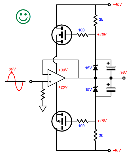
Here we see the top and bottom MOSFETs receiving their gate signal through a two-resistor voltage divider, rather than from the zener directly. This arrangement is the better approach as it is safer and grants us more options. Next, we see the buffer getting half of the 80V differential power-supply voltage.
The highest gate voltage the top N-MOSFET can see is 45Vpk, as the two-resistor voltage divider will split the zener voltage drop. With the buffer putting out 30Vpk, the following voltage relations obtain.
Conversely, with the output voltage swinging down to -30Vpk, we see the following voltage relations.
In both cases, the voltage drop across the buffer remains a constant 40V. It's all happy faces throughout. Now, let's return to cascoded power amplifiers.
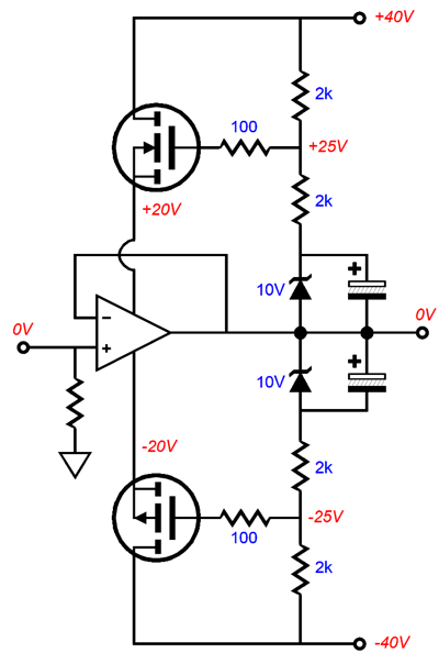
Crashing the Input Stage
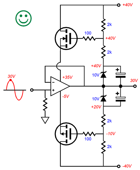
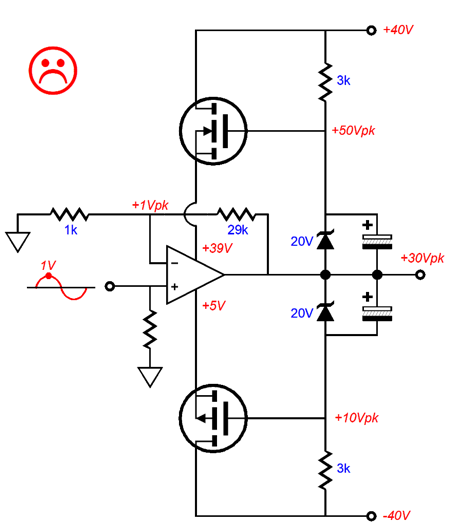
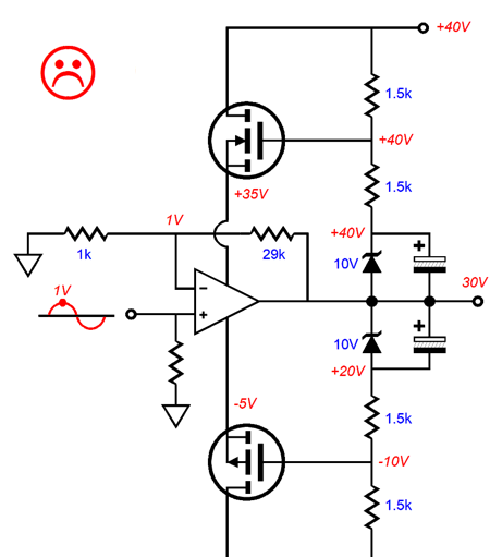
At idle, the amplifier sees bipolar power supply voltages of about +/-15Vdc. But as the output voltage climbs positively so, too, does the negative power supply connection. At the same time, the input signal might only rise by 1Vpk.
Here we see the amplifier putting out 30Vpk, but the negative power supply pin sees a voltage 4V more positive than its input signal. Not good—in fact, it's an impossibly bad situation. The amplifier's internal circuitry incurs a voltage overhead due to the constant-current sources and current mirrors and a cascoded or buffered input stage. With the LM3886, the minimum negative power-supply rail voltage is -10Vdc. If we try the cascode version that uses two-resistor voltage dividers to drive the MOSFET gates, we still end up shortchanging the LM3886 (although this might work with a different power amplifier).
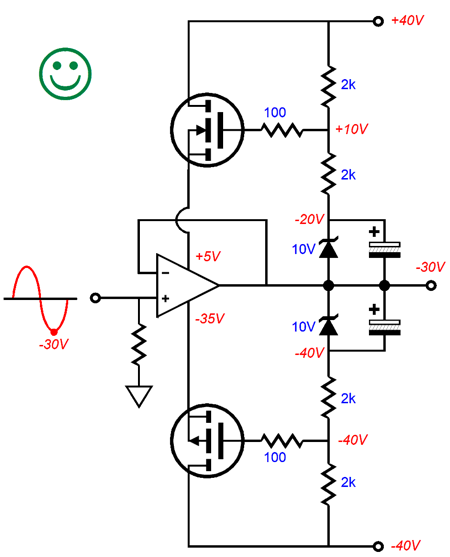
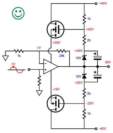
The workaround is to alter the two-resistor voltage divider ratio so that the negative power-supply rail voltage never falls below -10V.
With +30Vpk, the amp still gets -15V of negative power-supply rail voltage. Even with an impossible +40Vpk output voltage swing, the negative rail voltage would still be greater than -10V.
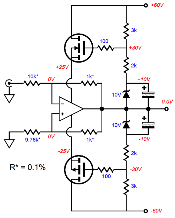
Amplifiers in Suspended-Supply Operation
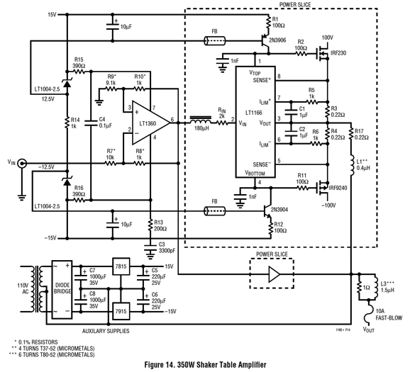
We have seen this topology here before; for example, in post 554 we saw the following schematic.
The shaker-table power amplifier runs its output MOSFETs on +/-100Vdc power-supply rails, but the low-voltage OpAmp (LT1360) is powered by floating +/-15Vdc power-supply rails. Yet, the amplifier's input is DC coupled at ground potential. The circuit magic-trick is introduced by the 9.1k and 1k two-resistor voltage divider resistors that span from the OpAmp's output to ground. Without these added resistors, the amplifier would run into the exact same input stage crashing as the cascoded amplifier ran into due to the negative power-supply rail voltage falling too low.
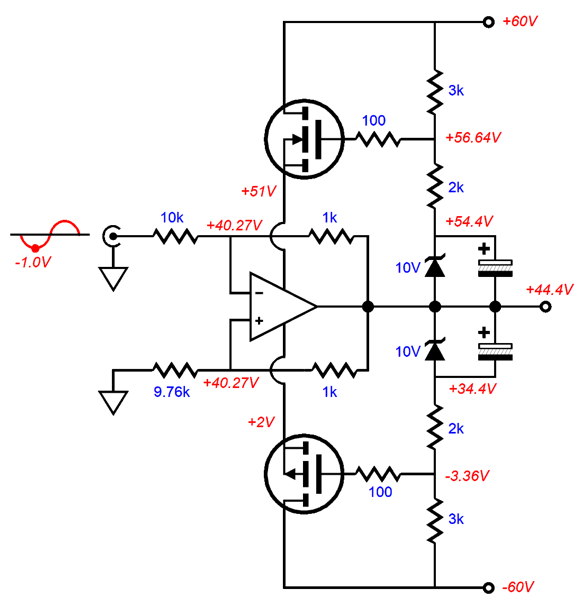
Here we see the amplifier using up less than half of the bipolar power supply differential voltage of 120Vdc (about 42%). With a +1Vpk of input signal, the amplifier output voltage swings down to -44.4Vpk.
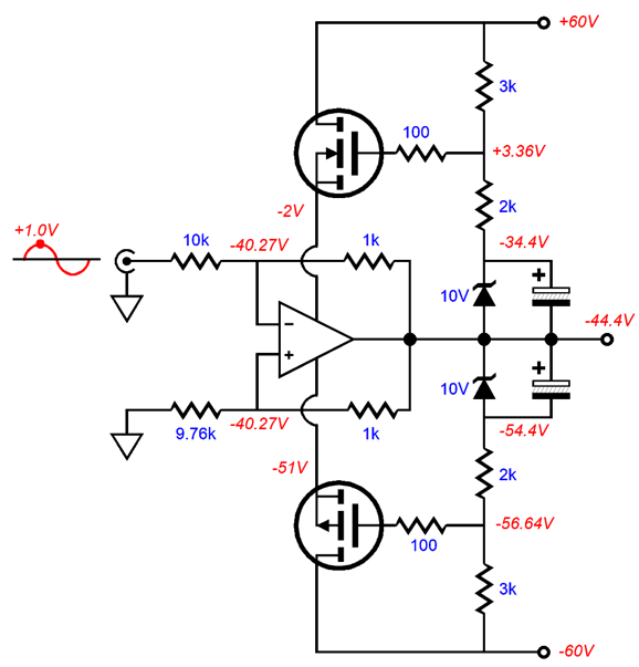
The power amplifier still sees a total voltage drop of close to 50V and both of its inputs are well within the +51V and +2V rail voltages. With a -1Vpk of input signal, the amplifier's output voltage swings up to +44.4Vpk.
The problem with suspended-supply operation is that it is a goosey affair that requires 0.1% resistor values and much patience and perseverance to stabilize at high frequencies. In addition, the input impedance is quite low. How low? In this example, the input impedance is not 10k, as it would be with a normal inverting amplifier, but a low 242 ohms. In other words, forget about using the typical tube-based line-stage amplifier to drive it. (Even if the line-stage amplifier held a robust cathode-follower output, the output coupling capacitor would have to be around 33µF to get a flat response down to 20Hz.) Well, couldn't we simply scale up all the resistor values by tenfold? We could try, but the input impedance would still be a crushing 2,420 ohms and things get squirrelly fast with higher value resistors.
Arrested Cascodes
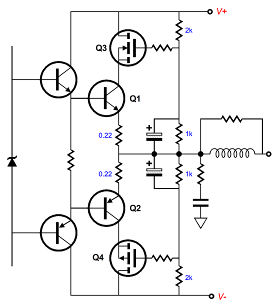
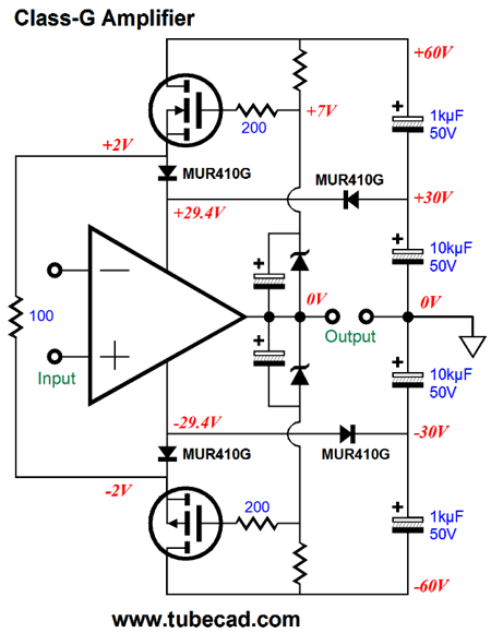
In the following, which is my improvement of class-G amplifier output stages, the top and bottom follower DO draw current at all times, albeit only little at idle. See posts 447 and 521 for more details. The schematic shows the 100-ohm resistor constantly providing a current path for the top and bottom MOSFET to draw current through, even at idle.
The amplifier runs off the inner, lower +/-30Vdc power-supply rails at idle and up to about 40W of output into an 8-ohm loudspeaker. The MOSFETs allow the rail voltages to expand, when output voltage swings greater than +/-26Vpk are needed, allowing the amplifier to deliver at least four times more power. Well, how do we alter an existing cascoded amplifier so that it encounters both a negative and positive power-supply-voltage limits? Here is one possible arrangement.
The added 15V zeners and two diodes allow one-way build-ups of rail voltage, while also imposing voltage stops. In the schematic above, we see the amplifier delivering 30Vpk (and 3.75A peak into an 8-ohm load), while its positive power-supply input swelled up to +35V, but its negative power-supply pin still sees -20.6Vdc, making a total of 55.6V of voltage differential. Okay, let's flip the input signal phase.
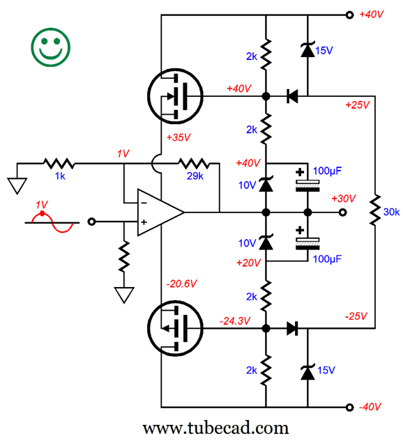
Now the amplifier's positive power-supply pin sees the truncated minimum voltage of a little over +20V. The 30k resistor supplies enough current flow through the two zeners to ensure that they achieve their expected break voltage. Here is a SPICE-generated graph that shows a two-cycle tone-burst at 1kHz.
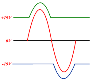
Sure looks like a class-G amplifier, doesn't it? Here the same test with a class-G output stage.
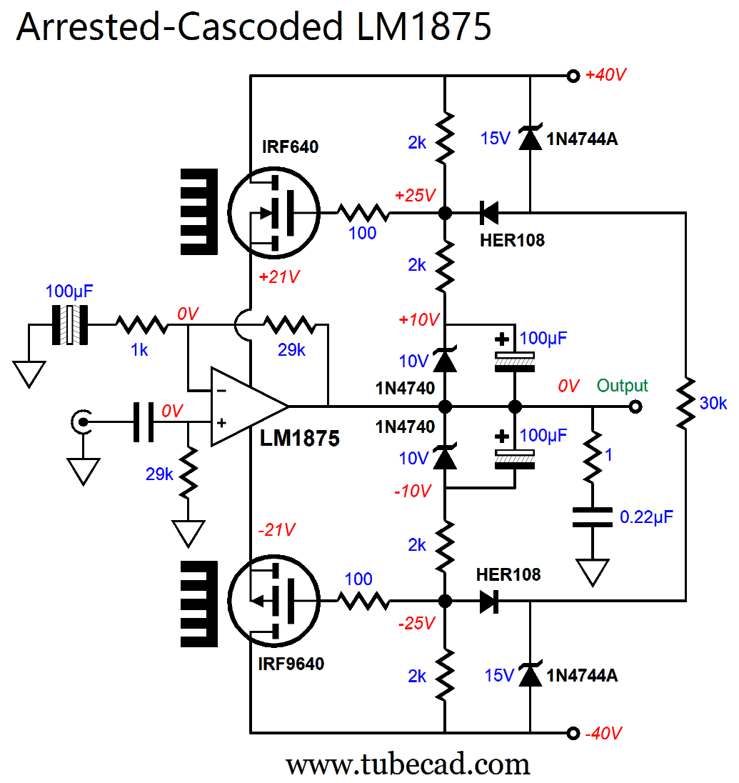
I used IRFP240 and IRFP9240 and OPA544 SPICE models. I was surprised that the OPA544 worked with power-supply rail voltage dips so far below +/-10V, as the data specifies a minimum differential power-supply differential voltage of 20V. (I have never completely trusted the OPA544 SPICE model, as it I have witnessed some weird behavior, such as a constant-current draw from the power-supply pins—in spite of 4A peak output swings. In addition, the distortion seems far too low.) Okay, here is completed example that uses the LM1875.
The MOSFETs used are TO-220 devices, like the LM1875, but with an amazing 125W power rating. The LM1875's power rating, with an infinitely big heatsink and at 25C, is about 42W. It's power-supply voltage limit is 60V differential or +/-30V. The bipolar power supply shown offers an 80V differential voltage, which would seem a no-no, but the cascoding limits the maximum voltage differential that the LM1875 will ever see to less than 60V. If you are wondering where the missing negative feedback capacitor is or why the output gets a Zobel network but no output inductor, the answer is that they didn't appear in the schematic provided by the LM1875 data sheet.
See: no capacitor across the 20k feedback resistor; no output inductor.
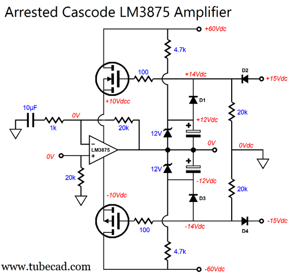
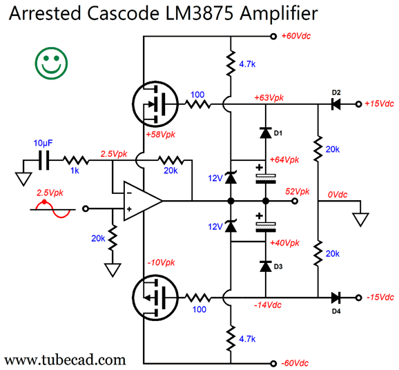
Arrested-Cascode LM3875 Amplifier By the way, I failed to mention in that last post that the LM3875 mounting tab, like that of the LM1875, is connected to its negative power-supply pin, which means ground potential with a single power-supply voltage; thus, we do not need to isolate the tab from the heatsink with a monopolar power supply. Here is what the LM3875 data sheet has to say:
Here is an arrested-cascoding of the LM3875.
No zeners attached to the power-supply rails this time; instead, we see diodes D2 and D4 attaching to a +/-15Vdc bipolar power supply (this power supply might be needed for an active crossover). The LM3875 sees +/-10Vdc bipolar power-supply voltages at idle. The LM3875 can idle as high as 70mA, but with the +/-10Vdc rail voltages, the dissipation would be only 1.4W at idle. Depending on the robustness of the raw power supply, the peak rail voltages should be close to +/-56Vpk. As the output swings positively, the top MOSFET follows along, thereby increasing the positive power-supply voltage.
A peak output voltage swing of 52V into an 8-ohm load results in 169W and 6.5A of peak current flow. This far exceeds the data-sheet limits for power and current output. The workaround is to use three LM3875 ICs in parallel.
The three amplifiers in parallel effectively see a 24-ohm load when driving an 8-ohm loudspeaker, which will third their required current output. An interesting question is: how should we calculate the power dissipation for an arrested-cascoded chip amplifier? With a power amplifier made up from discrete output transistors or MOSFETs, we would view the cascoded output-stage as a single entity. In the circuit shown above, the LM3875 amplifiers have it easy, as the rail voltages track the output signal with a 10V voltage cushion. In contrast, the top and bottom MOSFETs get hammered, as they effectively work within a +/-50Vdc rail voltages. In fact, we might have to double up on the MOSFETs to keep them cool enough. In this last design example, the amplifier sees +/-10Vdc rail voltages at idle, but which can inflate up to possibly +/-60Vdc rail voltages. I would take the average of these two voltage extremes; let us say +/-35Vdc as the rail voltages when doing the dissipation calculations for the chip amplifiers. Of course, the best practice is to work with reality, after doing some careful guesswork. When it comes to heatsinks, it pays to overestimate. But a lot depends on how hard the amplifier is driven. With high-efficiency loudspeakers, the outer MOSFETs may run cool; but with low-efficiency speakers or bass-heavy music, they might get toasty hot.
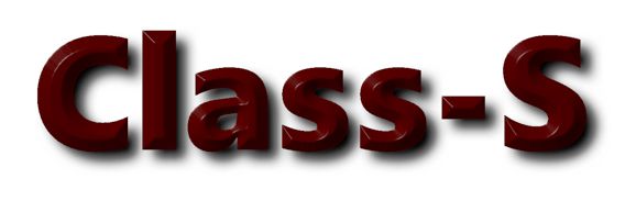
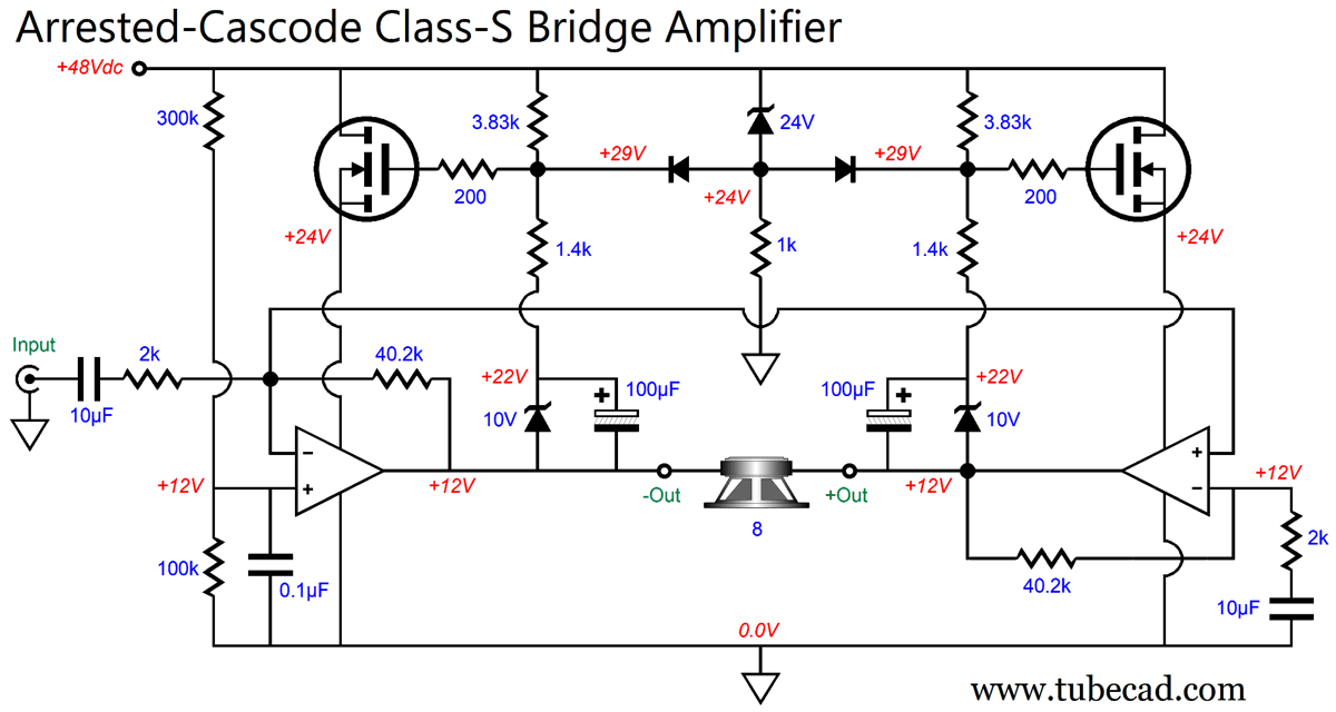
Arrested-Cascode Class-S Bridge Amplifier
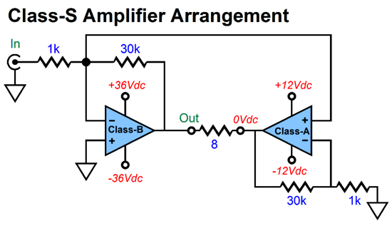
Mr. Aubrey M. Sandman introduced the world to his novel class-S amplifier designs in an article, "Avoiding conventional negative feedback by “error take-off” ," in the October 1974 issue of the great British electronics magazine, Wireless World. Then, in 1982 he produced a second article on the topic in Wireless World, whose newly detailed "H" or "bridge" approach to class-S operation was implemented in the Technics' Class-AA amplifiers of the 1980s. Here is the class-S amplifier "seed" circuit for an arrested-cascode bridge amplifier.
Since a loudspeaker is an intrinsically differential device, equal voltage at each terminal results in no cone movement whatsoever. Thus, if we applied the same amount of distortion, in phase, to both loudspeaker terminals the distortion cannot be "seen" by the loudspeaker driver. The class-A amplifier on the right acts as a virtual ground for the class-B amplifier's output, with the difference that the distortion produced by the amplifier on the left also appears at the class-A amplifier's output, thereby creating a distortion null in the loudspeaker. What happens if the class-B amplifier clips? Well, the clipped output is a form of distortion and the class-A amplifier will strive to make up the difference.
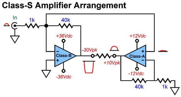
As far as the loudspeaker is concerned, no clipping occurred. In the schematic shown above, the class-A amplifier runs off of +/-12Vdc power-supply rails. What if, on the other hand, it ran off the same power-supply rails as the amplifier on the left, and what if both amplifiers were identical? The answer is that the amplifier on the right would still function as a distortion-reducing virtual ground, but when the amplifier on the left clipped, the right amplifier's output would compensate and extend the voltage swing across the loudspeaker up until the amplifier on the right also clipped. In other words, we would get four times more power output than the rail voltages would seemingly imply. The downside to such an arrangement is that the amplifier on the right would get far hotter than its partner would, as it would have to source and sink the same current flows as the amplifier on the left, but its output would still be at ground potential, so its output devices would see full bipolar power-supply voltages. Well, here is where cascoding could help.
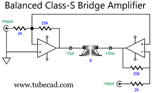
A monopolar power supply is used and the cascoding only applies to the amplifiers positive power-supply connections. The amplifier on the left can probably swing down 4V before clipping, making for a +/-8Vpk unclipped output as far as the loudspeaker is concerned. Thus, up to that +/-8Vpk voltage swing the amplifier on the right functions as a distortion-reducing virtual ground. At the same time, the amplifier on the left can probably swing positively up to about 42V without clipping, while the right amplifier's output remains locked at 12V. The loudspeaker sees a 30Vpk differential voltage, which implies 56W of average power. Once the amplifier on the left does clip, the amplifier on the right can swing down to 4V, possibly making for a 38Vpk voltage swing across the loudspeaker, thereby producing 90W of power. In contrast, a single amplifier working under the 48Vdc monopolar power supply could only deliver 25W of power output. In other words, we got close to a bridge amplifier's quadrupling of the power output. Why the shortfall? I assumed the cascoding will incur some losses. The arrested cascode action takes place due to the 24V zener and the two diodes, all of which limits the fall in the MOSFET's source voltages. If you find this tortuous circuit just too torturous, I will have to explain why I created it (other than just because I could). What I had in mind was using two LM3875 amplifiers, with their mounting tabs directly attached to the heatsink without any mica washer. If I cascoded the negative power-supply pins, then I would have to use the mica or silicon washer. In addition, I wanted to offload much of the heat dissipation to the MOSFETs. I would classify this design into the interesting-but-not-practical category. So why show it at all? You never know when a topology might be needed to solve what seemed to be an intractable problem. The more tools in our toolkit, the better chance we have of fixing some difficulty. Let's return to Mr. Sandman's class-S operation with two amplifiers. Although it might seem obvious that we can create a balanced version, I do not believe that I have ever mentioned it before. Let me correct that omission.
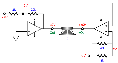
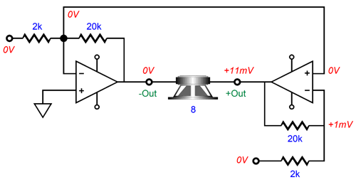
This bridge amplifier requires a balanced set of input signals (+ and – in other words). Here is an example of how it works with an input signal of +/-1V.
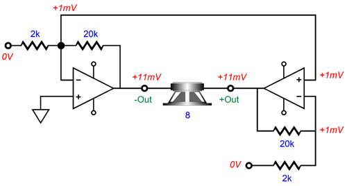
Each inverting amplifier amplifies and inverts its input voltage at its output, resulting in the 20V voltage drop across the loudspeaker. If both amplifiers delivered distortion-free output, this bridge amplifier would perform no differently from any other bridge amplifier with a balanced input signal. Okay, but what if there is some distortion, what happens then? A DC offset voltage on the left amplifier is a form of distortion, albeit DC distortion.
The 11mV DC offset voltage is reduced by the two-resistor voltage divider formed by the 2k and 20k negative feedback resistors to 1mV at the left amplifier's inverting input, which is also the right amplifier's non-inverting input. The right amplifier sees the 1mV voltage as signal to amplify, which it does by 1:11, as that is its non-inverting gain. Since, the loudspeaker sees 11mV at both of its terminals, it completely ignores the voltage offset. The speaker could see 11kV or 11 megavolts at both terminals and still not "see" the voltage. Differentially, no difference means zilch. In SPICE simulations, I witnessed a reduction in forced distortion of about -40dB with this class-S bridge-amplifier configuration over the standard bridge amplifier. This assumed a perfect amplifier on the right. Note that the distortion produced by the amplifier on the right is not nulled by the amplifier on the left. For example, if the DC offset appeared on the right amplifier's output, the loudspeaker would see it.
How can the amplifier on the right have its inputs at different voltages? There are several possibilities, such as mismatched input FETs (or transistors) or a heat differential between the input devices. In any case, the amplifier on the left does nothing to counter the DC offset.
Music Recommendation: Third Coast Percussion, Perspectives I have mentioned this before but it is worth repeating: the line that separates jazz from classical music is fuzzy. In many ways, American jazz music is modern classical music. One definition of classical music is that is music that bears repeated listening over decades and centuries. I promise you that 1,000 years from now Bach's music will continue to please and astound. The same can be said of great jazz music from Duke Ellington and other giants of the jazz pantheon.
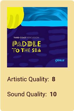
Third Coast Percussion is an ensemble of four extremely talented percussionists. What is the Third Coast? In the USA, we have three major coasts, the East Coast, the Left Coast (formerly, the West Coast, but formally Left ;), and the Mid Coast, the last of which is the one that our Second City, Chicago, looks out upon, i.e. Lake Michigan. Another album I enjoyed by the ensemble was Paddle to the Sea.
In a review by David Hurwitz at classicstoday.com, he gives the album a rating of
My rating would be two 9's. The third album I listened to was Archetypes, which was also delightful. I do not know if these three albums are the group's strongest, but they were all high-res.
//JRB
Did you enjoy my post? Do you want to see me make it to post 1,000? If so, think about supporting me at Patreon. The more support I receive, the more I can post.
User Guides for GlassWare Software
For those of you who still have old computers running Windows XP (32-bit) or any other Windows 32-bit OS, I have setup the download availability of my old old standards: Tube CAD, SE Amp CAD, and Audio Gadgets. The downloads are at the GlassWare-Yahoo store and the price is only $9.95 for each program. http://glass-ware.stores.yahoo.net/adsoffromgla.html So many have asked that I had to do it. WARNING: THESE THREE PROGRAMS WILL NOT RUN UNDER VISTA 64-Bit or WINDOWS 7, 8, and 10 if the OS is not 32-bit or if it is a 64-bit OS. I do plan on remaking all of these programs into 64-bit versions, but it will be a huge ordeal, as programming requires vast chunks of noise-free time, something very rare with children running about. Ideally, I would love to come out with versions that run on iPads and Android-OS tablets.
|
I know that some readers wish to avoid Patreon, so here is a PayPal button instead. Thanks.
John Broskie
John Gives
Special Thanks to the Special 80 To all my patrons, all 80 of them, thank you all again. I want to especially thank
All of your support makes a big difference. I would love to arrive at the point where creating my posts was my top priority of the day, not something that I have to steal time from other obligations to do. The more support I get, the higher up these posts move up in deserving attention.
If you have been reading my posts, you know that my lifetime goal is reaching post number one thousand. I have 432 more to go. My second goal was to gather 1,000 patrons. Well, that no longer seems possible to me, so I will shoot for a mighty 100 instead. Thus, I have just 20 patrons to go. Help me get there. Thanks.
Support the Tube CAD Journal & get an extremely powerful push-pull tube-amplifier simulator for TCJ Push-Pull Calculator
TCJ PPC Version 2 Improvements Rebuilt simulation engine *User definable
Download or CD ROM For more information, please visit our Web site : To purchase, please visit our Yahoo Store: |
|||
 Versus


%20LM3875%20Amplifier%20Large.png)


| www.tubecad.com Copyright © 1999-2023 GlassWare All Rights Reserved |