| John Broskie's Guide to Tube Circuit Analysis & Design |
| 22 March 2014
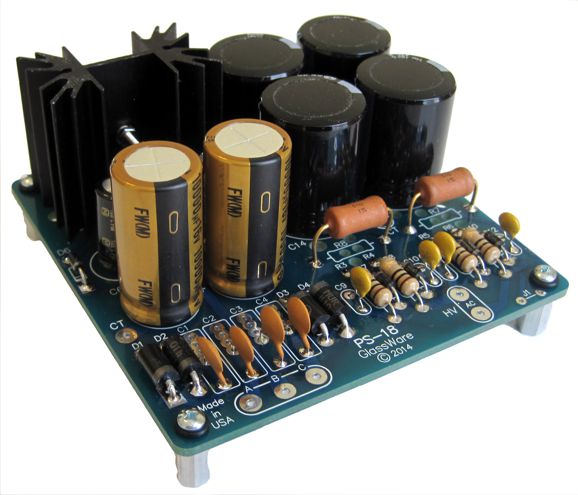
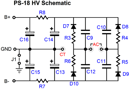
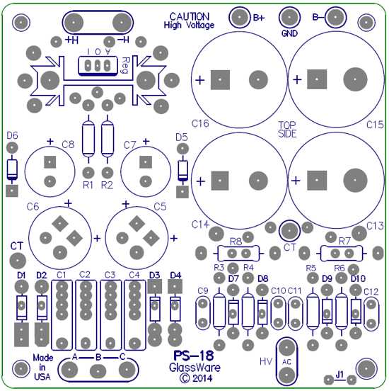
New Bipolar High-Voltage Power Supply
PS-18 Bipolar Power Supply Kit
The boards are small, being only 4in by 4in, but pack quite a wallop due to the large-valued capacitors used. Two RC-based pi filters smooth the bipolar DC outputs.
The heater power supply is regulated and can accept either a full-wave-bridge or voltage doubler or full-wave center-tapped rectifier configuration.
The PS-18 bipolar power-supply kits comes with either 470µF/250V or 150µF/400V capacitors. The PCB is made from the same high-standard extra-thick, 2oz copper, double-sided board, with solder masks and silk screen part placement labels on both sides. As one customer put it, "You could make a bullet-proof vest out of your PCBs." The PS-18 kit is available now at the GlassWare-Yahoo store.
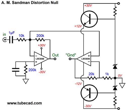
More A. M. Sandman Circuits
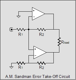
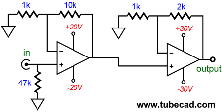
The top amplifier is configured in the inverting mode. Any distortion it produces at its output will appear at its inverting input, but reduced by the ratio set by resistors R1 and R2, so ratio equals R1/(R1 + R2). This sampling of the output distortion is then fed to the bottom amplifier's non-inverting input, so it gets amplified in phase by the amplification ratio set by (R1 + R2)/R1. If the top amplifier produces no distortion, which would include clipping, the bottom amplifier's output would effectively replace a connection to ground, as no signal would be present on its output. But if the top amplifier clips, putting out only 20Vpk of the waveform's true 25V peak, the bottom amplifier's output will swing 5Vpk to make up for the missing voltage. In other words, top amplifier nominal output wattage could effectively quadruple, if the top and bottom amplifiers and power supply are up to the task. On the other hand, even if we limit the top amplifier to just its nominal power output, the bottom amplifier doesn't coast along, as it must source and sink just as much current as the top amplifier can dish out. This can be a problem, as the bottom amplifier's output would remain at 0V, so its output devices would dissipate much more heat than the identical top amplifier would develop. For example, if the top amplifier swings 24Vpk and 3Apk into an 8-ohm speaker, and if the power-supply rail voltages are +/-30Vdc, the top amplifier's output devices will see at the peak 30V - 24V, or 6V at 3A. The bottom amplifier, on the other hand, will see the full 3A of current flow and the full 30V of power-supply rail voltage, so its peak dissipation must five times higher, as 30V is five times greater than 6V. In other words, the bottom error-takeoff amplifier must get hotter than the top amplifier. Alas, heat is the enemy of solid-state devices. If discrete parts were used in making the two amplifiers, this would not be that big a deal, as the bottom amplifier could hold either more output devices or a larger heatsink or both. But with an OpAmp amplifier, i.e. IC chip amplifiers (gainclone) amplifiers, this option is not really available to us. One workaround would be to use a separate lower-voltage power supply for the bottom amplifier. (For exxample, a custom power transformer could be made with many taps on its secondary.) Or, we could use a single power supply, but limit the voltage that the bottom amplifier gets to use.
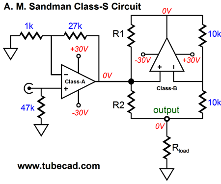
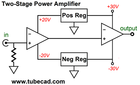
The top amplifier sees the full ±30V rail voltages, but the bottom amplifier only sees ±12V, as the two power transistors act as voltage regulators of sorts (capacitance multipliers). I like this setup, although it will not greatly increase the potential power output, as it helps ensure that the bottom amplifier cleanly reproduces the top amplifier's distortion. And my primary goal would be low distortion rather than more power. (Bear in mind that the above schematic is the stripped-down version, as many supporting parts are missing, such as large capacitors shunting both zeners and Zobel networks on the amplifier outputs.) In my last post, we saw Dr. Sandman's class-S scheme, wherein a small-power class-A amplifier drives and corrects a class-B amplifier's output.
The assumption has been that resistors R1 and R2 are the same value. But what happens if they aren't? For example, what if R1 is twice as large as R2? In this example, the circuit will function as an impedance-multiplier circuit, so the class-A amplifier will effectively work into a load impedance equal to twice the actual speaker impedance. The formula is as follows: Effective Rload = R1/(R1 - R2) What happens if R1 is smaller than R2? In that case, the impedance would go negative, which means that the class-A amplifiers output current would subtract from the class-B amplifier's, so the output the speaker sees would fall. One conclusion is that if we want the class-A amplifier to see the highest impedance load, we should use tightly matched resistors for R1 and R2.
OTL Power Amplifier Design
This OTL requires a differential (balanced) input signal, which a long-tailed differential amplifier can provide. With a few alterations, a bipolar power supply could be used, so that the big coupling capacitors would no longer be needed. (Well, at least in theory; I like the idea of the big coupling capacitors protecting my speakers from a device failure, such as a shorting tube.) Recently, I was looking in an old electronics book, Henney's Radio Engineering Handbook, where I found the following three OTL designs. DANGER! DANGER! DANGER!
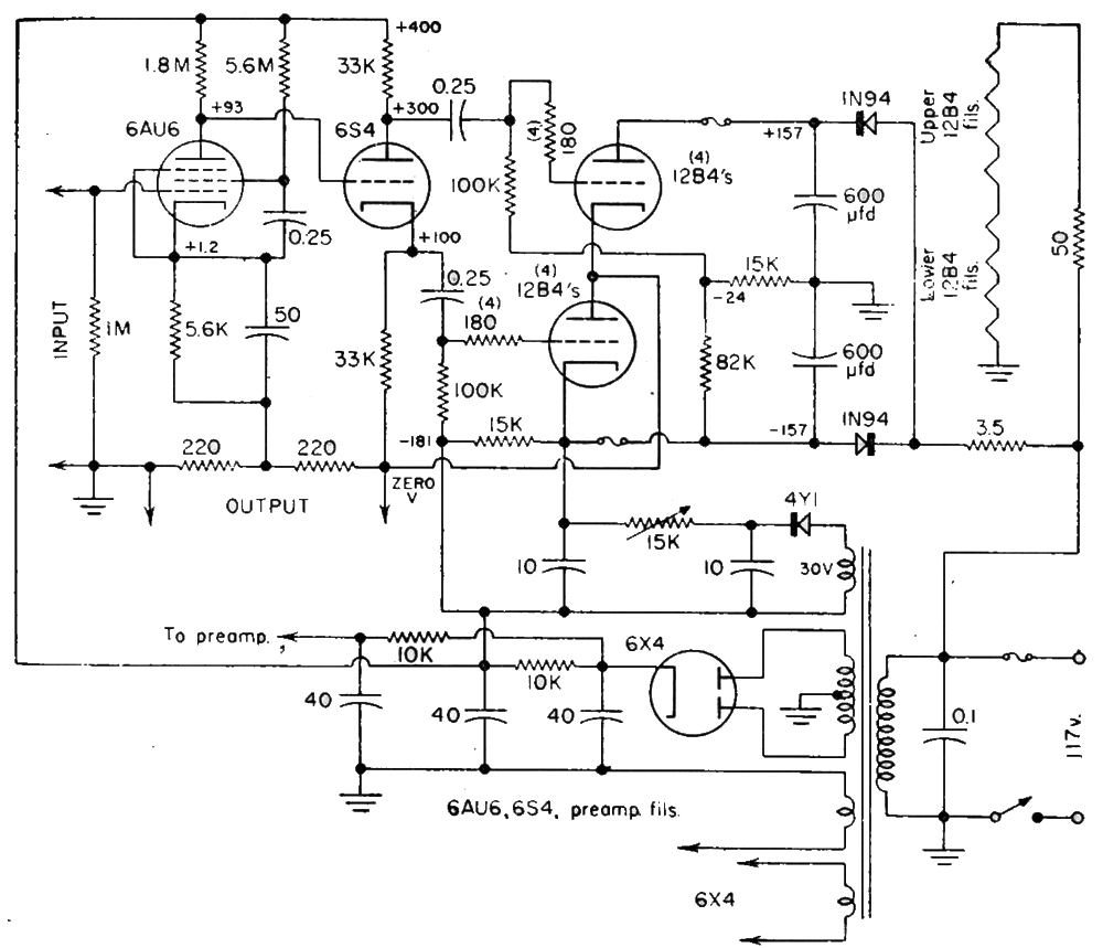
A 6AU6 pentode-based input stage provides the voltage gain. Next, a 6S4-based split-load phase splitter feeds the two sets of opposing triodes their required input signal. A negative feedback loop lowers the gain, distortion, and output impedance. Both top and bottom output triodes function as grounded-cathode amplifiers, which explains why the split-load phase splitter's cathode resistor terminates into the OTL's output. All in all, not a bad design. Amazingly enough, the next OTL design is just as as scary as the the first one.
Don't see it? Look at the DC voltage at the outputs. Those were the days: when men were men and cats and dogs often died from chewing on speaker cables. Note how the phase splitter offers four outputs. Why? The balanced output stage has the top triodes functioning as cathode followers, but the bottom triodes function as grounded-cathode amplifiers, so the top triodes must see a much larger input signal than the bottom triodes. Just what the ratio must be depends on the output tubes used and the load driven. The next OTL design is truly interesting, but also dangerous, as it, like the first OTL design, forgoes all power transformers and rectifies the raw wall AC voltage for all the triodes; even the tube heaters are thrown across the outlet's AC voltage, making this a truly transformer-less amplifier.
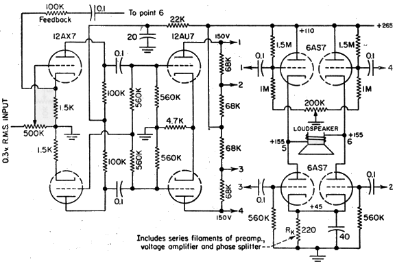
Note the two negative feedback loops, one just for the two first triodes and one that starts the output and terminates right at the cathode of the third triode from the left. In other words, the first two triodes constitute a voltage amplifier that develops all the voltage gain, then all the remaining tubes create a unity-gain buffer! If you do the math, you realize that the lowest possible distortion occurs with only one global feedback loop that encompasses all the stages. But harmonic distortion is only one ill that may befall a power amplifier. For example, a power amplifier might randomly oscillate or clip in a grotesque fashion. When I was in college, I designed all my solid-state power amplifiers with two feedback loops and two gain blocks. Both amplifier stage consisted of two internal stages, which brought the total to four stage; in contrast, a typical transistor amplifier holds three stage. But as each feedback loop in my design only had two stages to encompasses, not three, my two gain blocks were quite stable.
In other words, I gave up a little distortion reduction for increased stability and better recovery from clipping. In addition, the two stage approach allowed me to offer the first gain stage regulated power-supply rails.
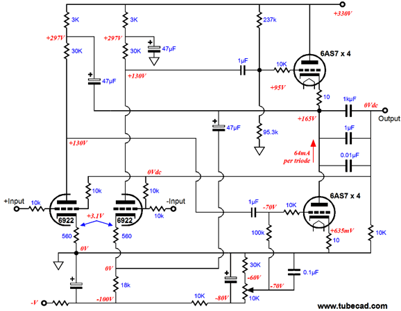
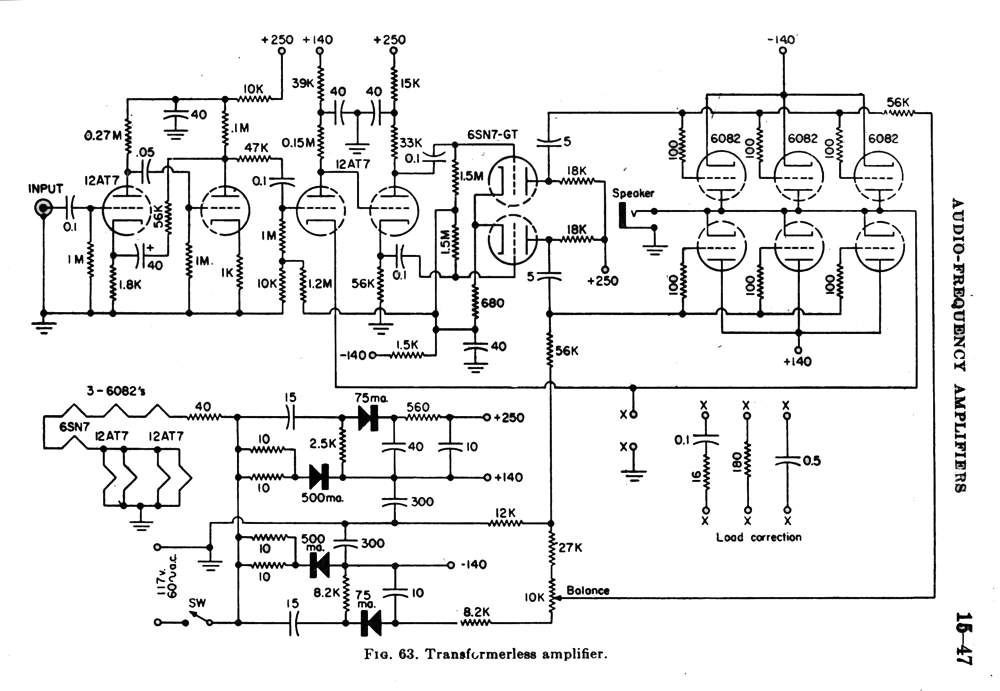
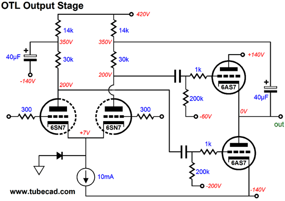
At first, I took the lazy route and I tried a simple zener shunts to reduce the rail voltages for the first amplifier, but I felt that it just wasn't good enough; I was right. Adding voltage regulators, LM317 & LM337 types, made a dramatic improvement in imaging and hall ambience reproduction. Note how the first age is never required to produce more than +/-8V of peak voltage swing at its output, as the second gain stage's gain of 3 will amplify it up to +/-24Vpk of output. This setup established a nice feature: while the second amplifier could and would clip, the first amplifier never (or seldom) did. Returning to this last OTL design, the potentiometer labeled "Balance" doesn't actually adjust the balance between the input signals for top and bottom output triode, but the DC offset. As for current-swing balance between top and bottom triodes, other than the high amount of negative feedback, the only mechanism for giving the bottom output triodes, whose cathodes attach to the -140V rail, less input signal is the dissimilar plate and cathode resistors in the split-load phase splitter, 33k and 56k. This is a rather clunky workaround, but it works fairly well due to the 6AS7's amazingly low mu, namely 2. If the triode offered a mu of 20, then this simple trick would certainly fail to impress. In short, what is needed is a way of adding the OTL's output signal to the signal that the top triodes see from the differential amplifier, which will cause the top triodes to function as grounded-cathode amplifiers, just like the bottom triodes. The easiest way to do this is with a capacitor that spans from the output to the phase splitter, as shown below. With this connection in place, both top and bottom output triodes see the same cathode-to-grid signal amplitude and offer the same output resistance, effectively the triode's rp. But once the feedback loop is put in place, the OTL's output falls significantly.
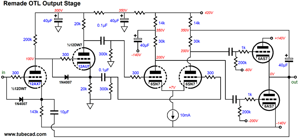
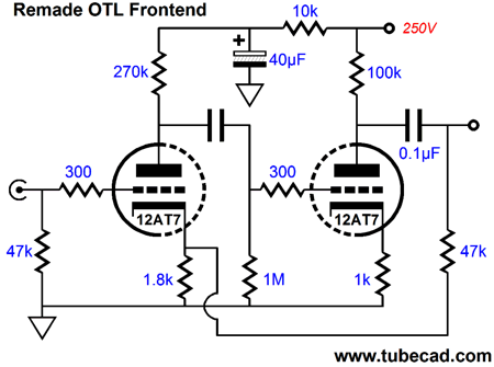
Another problem with the old design, other than the obvious safety issues, is that its bottom output triodes, whose cathodes attach to the -140V rail, see 100% of the negative power-supply rail ripple, but their grids do not any of this noise, which means that in the absence of the heavy feedback ratio, this amplifier would hum along with the ripple. (To be frank, many high-end-audio if not all high-end-audio OTL amplifiers sold today suffer from this defect.) The workaround, as I described her many times before is to superimpose the negative power-supply-rail noise on the signal that the bottom triodes sees. In the schematic above, note where the leftmost 40µF capacitor terminates; it's not ground, as 99.9999% of high-end-audio OTL amplifiers sold today would do. For more information on OTL output stage balance and PSRR enhancement, read this PDF that I wrote back in 2001; but do not get confused by the squares labeled with an "N" as these simply signify either a triode or a pentode or an N-channel MOSFET... I would redo the the rest of the unity-gain power buffer. For example, I would use a 12DW7/ECC832 instead of the 12AT7 used in the original. Why? The 12AX7 triode within the dissimilar tube offers more gain and its partner 12AU7 triode can draw more current; besides, I like the JJ ECC832. Rather than terminate the input triode's cathode into the OTL's output directly; instead, I would use a coupling capacitor, as it frees us from critical input DC issues. The next step is to put everything together, as shown below.
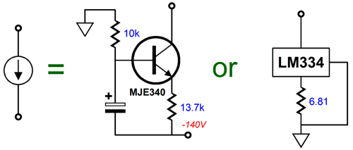
I used a constant-current source in the above schematic, which no doubt made some readers nervous. Why? You cannot readily order a high-voltage constant-current source from Mouser.com or pick one up at Radio Shack, alas. Still, building a solid-state-based constant-current source is no big deal, as single NPN transistor is all that is needed, along with two resistors and a capacitor. Alternatively, we could ignore the negative power-supply rail and just ground an LM334 constant-current source.
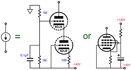
Of course, may would prefer to keep an all-tube design going, so the following tube-based constant-current sources are also usable.
The 6DJ8 triodes in cascode present a fairly high impedance (roughly, rp + (mu + 1)(rp + [mu + 1]Rk), as would a pentode's plate. By the way, note how we progress backwards in an amplifier design, starting with the output tubes, moving back to the input stage. This brings us to the two-stage input stage, which defines a standalone amplifier, with its own negative feedback loop. Note, below, how I have eliminated the 40µF electrolytic coupling capacitor that the 47K feedback resistor used in the original design. Wonderful, but now this amplifier has a DC offset at its output equal to the input tube's cathode voltage. This would be a no-no for a line stage amplifier, but it little matters to the unity-gain power buffer's input, because of its 143k cathode resistor, which readily absorbs this small DC offset. (I tried to retain as many of the original part values as possible. In reality, I would use different values for the plate and cathode resistors. Actually, I would probably use an Aikido amplifier instead.)
As always, I had much more to say. Here is the what the old book had to say about the OTL circuit:
Next Time
For those of you who still have old computers running Windows XP (32-bit) or any other Windows 32-bit OS, I have setup the download availability of my old old standards: Tube CAD, SE Amp CAD, and Audio Gadgets. The downloads are at the GlassWare-Yahoo store and the price is only $9.95 for each program. http://glass-ware.stores.yahoo.net/adsoffromgla.html So many have asked that I had to do it. WARNING: THESE THREE PROGRAMS WILL NOT RUN UNDER VISTA 64-Bit or WINDOWS 7 & 8 or any other 64-bit OS. I do plan on remaking all of these programs into 64-bit versions, but it will be a huge ordeal, as programming requires vast chunks of noise-free time, something very rare with children running about. Ideally, I would love to come out with versions that run on iPads and Android-OS tablets.
//JRB |
I know that some readers wish to avoid Patreon, so here is a PayPal button instead. Thanks. John Broskie
Kit User Guide PDFs
E-mail from GlassWare Customers
High-quality, double-sided, extra thick, 2-oz traces, plated-through holes, dual sets of resistor pads and pads for two coupling capacitors. Stereo and mono, octal and 9-pin printed circuit boards available. 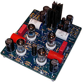 Aikido PCBs for as little as $24 http://glass-ware.stores.yahoo.net/
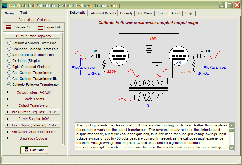
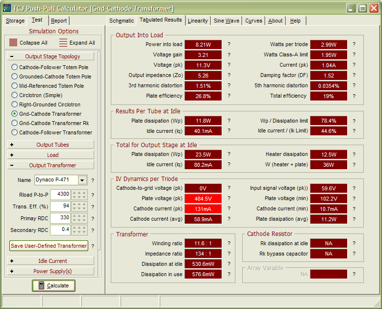
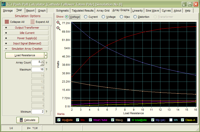
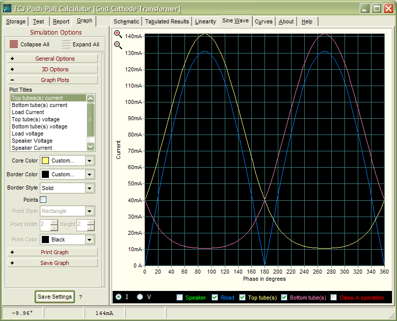
Support the Tube CAD Journal & get an extremely powerful push-pull tube-amplifier simulator for TCJ Push-Pull Calculator
TCJ PPC Version 2 Improvements Rebuilt simulation engine *User definable
Download or CD ROM For more information, please visit our Web site : To purchase, please visit our Yahoo Store: |
|||


| www.tubecad.com Copyright © 1999-2014 GlassWare All Rights Reserved |