| John Broskie's Guide to Tube Circuit Analysis & Design |
17 October 2021 Post Number 546
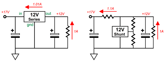
More Shunt Regulators
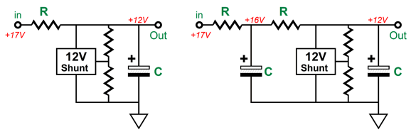
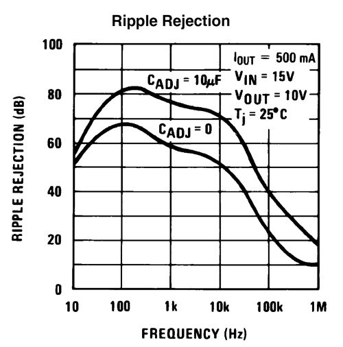
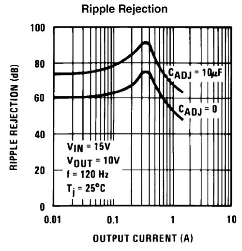
Imagine each channel getting its own shunt regulator. Now, imagine sound in only one channel. What appears in the other channel? Possibly nothing, as the shared raw B+ voltage never sees a music-induced current variation. In contrast, the series regulator will pass on the varying current flow and it could find its way into the other channel. Even in a mono amplifier, the shunt regulator can prevent one stage from being influenced by other stages. In addition, the shunting capacitor has a lot less work to do if there is a constant-current draw. One advantage that passive filters have over active filters is that a passive filter does not run out of gain at high frequencies; active filters do. Moreover, active filters are necessarily voltage-limited. We cannot buy a 10kV OpAmp, but we can buy a 10kV capacitor. Well, the shunt regulator comprises a passive low-pass filter in the form of the series resistor (R) and the shunting capacitor (C). Indeed, we can use two resistors in series in place of the single series resistor; and add an additional capacitor to pre-filter the DC entering the shunt regulator. The added capacitor can be as small as 0.1µF. It should, however, be a high-quality type. By the way, I have found that all voltage regulators, whether they be low-voltage or high-voltage, series or shunt, benefit from some pre-filtering. If we exam the datasheet for an IC voltage regulator, we see that its peak PSRR (often referred to as "ripple rejection" in the datasheets) occurs at around 120Hz, which is the ripple frequency in countries that use 60Hz wall voltages. Here is the graph for the LM317. Another by the way, most do not know that the peak PSRR depends on the amount of current passed. Here is the graph for the LM317.
In other words, the specified PSRR of 80dB will prove to be only 60dB with a 20mA load, say an OpAmp-based phono preamp. Let's say that we are willing to lose a 1 volt voltage drop across a pre-filter series resistor. With the trivial load of 20mA, we can use a 47-ohm resistor and use a 4.7kµF pre-filter shunting capacitor. The resulting -3dB low-pass frequency for the pre-filter is 0.72Hz, with its output at 100Hz being down by -43dB.
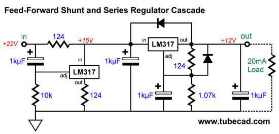
We add this attenuation to the regulator's -60dB and get -103dB. Beyond enhanced PSRR, the pre-filter rounds off the sharp edges of the power-supply noise entering the voltage regulator, which greatly unloads the regulator. I have found that a pre-filter made up of a 10-ohm resistor and 0.1µF capacitor makes otherwise flaky high-voltage regulators rock stable. Before leaving the LM317 behind, here is an idea for an ultra-clean low-voltage regulator that uses two LM317s, but in different ways.
The LM317 on the left is configured as a feed-forward shunting regulator that kills the raw power-supply ripple by drawing an in-phase current relative to it. Note the leftmost 1kµF capacitor, which relays 100% of the ripple noise to the LM317's adjustment pin, which in turn the LM317 imposes upon the 124-ohm resistor at its output. Say the raw B+ voltage swells up 1Vpk, the bottom 124-ohm resistor will see this 1Vpk and draw 1/124 more current as a result, causing the top 124-ohm resistor to see a 1Vpk greater voltage drop, which will undo the voltage swell, as 1V - 1V = 0V. The top 124-ohm resistor and the 1kµF capacitor at its right form an RC filter with a -3dB transition frequency of 1.3Hz. In other words, the LM317 on the right, which is configured as a series regulator, gets a very clean DC input voltage.
Bastode Series Regulators
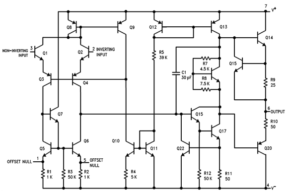
The first time I saw the bastode topology was I the now ancient LM741 OpAmp.
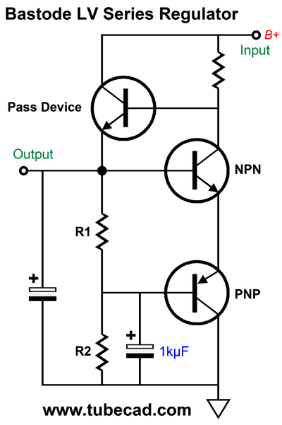
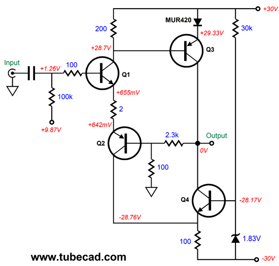
I thought I understood solid-state electronics well enough, but I could not make sense of how transistors Q1 through Q4 worked. At first glance, transistors Q1 and Q2 look like they form a conventional differential amplifier pair; they don't. After some head scratching, it made sense. Transistors Q1 and Q3 do form a differential amplifier, but not a conventional one; the same holds true for transistors Q2 and Q4. As the voltage differential between the top NPN and bottom PNP transistor bases increases, the greater the current flow through the transistors; as the voltage differential decrease, the less the current flow. Unlike the conventional transistor-based differential amplifier, the bases in the bastode differential amplifier cannot be at the same DC voltage, due to the base-to-emitter voltage drops. This can be deemed either a feature or a bug, depending on the application. In the series voltage regulator, it is a feature, as it grants us a free voltage reference. Here is a low-voltage example.
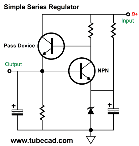
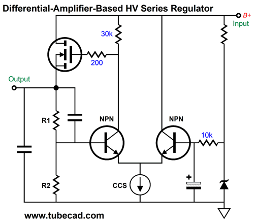
The base-to-emitter voltage drops add up to about 1.2 volts. Thus, resistor R1 will see a 1.2V voltage drop and its resulting current flow will also flow through resistor R2 to ground. The voltage drop across resistor R2 must be added to the 1.2V drop across R1 to get the final regulator output voltage. If the regulator's output voltage becomes dragged down, the bastode transistors will draw less current, causing the pass device's base voltage to rise, thereby lifting the output voltage back to the target voltage. Conversely, if the output voltage rises above the target voltage, the bastode transistors will draw more current, causing the pass device's base voltage to fall, forcing the output down to the desired output voltage. In a nutshell: negative feedback. Remember, all voltage regulators require three things: a voltage reference, a pass device, and a negative feedback system. This simple bastode-based voltage regulator holds all three. We can make an even simpler series voltage regulator. It must abide by the essential three components: a voltage reference, a pass device, and a negative feedback system. In other words, we need at least two active electronic devices and voltage reference. The zener plays the part of the voltage reference, with a large-valued shunting capacitor to dampen the zener noise. The NPN transistor sees the zener voltage at its emitter and compares it to the voltage at its base. If the regulator's output voltage droops, the NPN transistor will slacken off in its current flow, which will cause pass-device NPN transistor's base voltage to increase, thereby forcing a greater current conduction, which will in turn pull the output voltage back up to the target voltage. The resistor that bridges the B+ voltage to the zener is there to ensure that the zener breaks at the desired voltage and to allow the NPN transistor to use a larger-valued collector resistor. The resistor that bridges the output to ground is there allow some idle current to flow through the pass device. Let's take a brief detour before returning to the bastode circuits. I stated that the bastode was a vertical differential amplifier, not the typical horizontal or lateral differential amplifier. Well, let's look at a high-voltage series regulator based on the typical differential amplifier.
The N-channel MOSFET is the pass device, while the zener provides the voltage reference and the two NPN transistor arranged as a differential amplifier provide the negative feedback mechanism. The constant-current source is an embellishment, as a shared emitter resistor could have been used. Resistor r1 and R2 set the output voltage. The capacitor shunting R1 undoes the two-resistor voltage divider form by R1 and R2, at least at high frequencies. The 10k resistor and the electrolytic capacitor form an RC filter that cleans up the zener voltage drop. The differential amplifier strives to maintain the same voltage at each transistor base. So if the output voltage droops, the left transistor's base will see less base voltage than the right transistor, causing the MOSFET to see a higher gate voltage, as the left transistor will decrease its current conduction, lifting the output voltage up to sufficiently to bring the two base voltages inline. We can get fancier still by using a current mirror at the top of the differential amplifier.
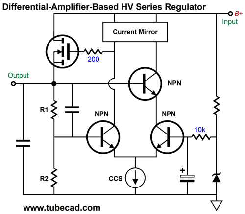
The current mirror greatly improves the PSRR and the differential amplifier's linearity. Moreover, it creates a push-pull drive for the MOSFET's gate. In other words, the gate can be both pulled up actively and pulled down actively. The extra zener just soaks up voltage so both transistors see roughly the same emitter-to-collector voltages. Adding this extra zener assumes a fixed raw DC power-supply voltage. An alternative arrangement might be to add an extra NPN transistor instead, creating a cascode flourish.
I haven't run this regulator design in SPICE simulations, but it looks promising. The limitation to the current mirror is that it necessarily requires the use of two PNP transistors, which top out at -500V for the emitter-to-collector voltage limit; for example, the ZT560 . Okay, we return to the bastode-based high-voltage series regulator.
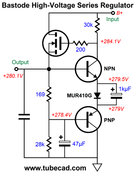
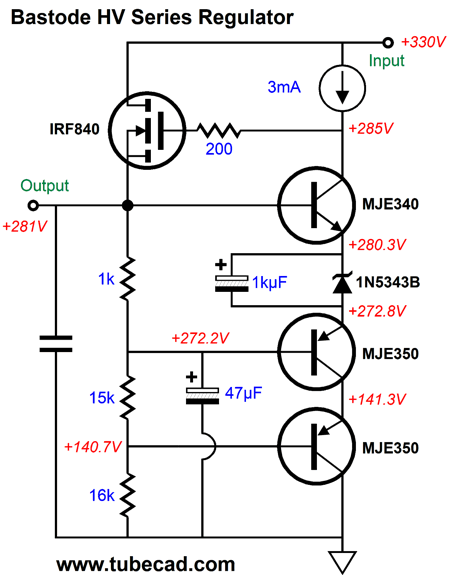
The pass device is a high-voltage MOSFET rather than a NPN transistor. Why? In general, MOSFET are more robust than bipolar transistors. In addition, they are available in much higher voltages. For example, we can buy a NPN power transistor, the MJW18020G, with a 1kV emitter-to-collector breakdown voltage; alas, its sustained breakdown voltage is only 450V. On the other hand, a variety of 800V NPN transistors exist, as they were needed for the horizontal deflection circuits in CRT monitors and TVs, along with electronic ballast for fluorescent lighting. The problem with these readily available devices is that their current gain (HFE) is woefully low, often as low as 10. In other words, if we are going to get a current flow of 200mA from the emitter, we must deliver 20mA into the base. In contrast, high-voltage 1kV MOSFET, such as the IRFPG30 in the TO-247 package and rated for 125W, cost only a few dollars and requires no static drive current. (If you must switch it on and off at supersonic high frequencies, then you must overcome the 1nF of input capacitance with current, as charging and discharging capacitance requires current.) The reference voltage is the sum of the two base-to-emitter voltages, about 1.2V to 1.4V. The 47µF capacitor shunts resistor R2 and provides an AC connection to ground for the PNP transistor. Think of a voltage regulator as a unity-gain amplifier that delivers a desired DC offset and whose input signal is ground. Resistors R1 and R2 set the output voltage and provide a current path for the MOSFET's idle current flow. One problem this series regulator faces is that the reference voltage is tiny compared to the output voltage. We can make the reference voltage a bit larger by adding a diode.
The diode's voltage drop is added to the two base-to-emitter voltages. We can go even further and replace the diode with a zener diode or an IC voltage reference.
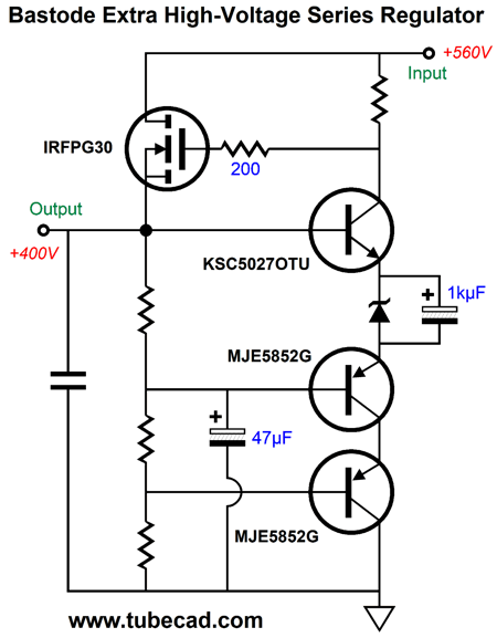
Yes, I did slip in a further enhancement: the extra PNP transistor, which doubles the PNP transistor's voltage limit (400V for the MJE5852G). Like the diode in the previous schematic, the zener is shunted by a large-valued capacitor. Here is a slightly lower-voltage design example.
The collector resistor has been replaced by a constant-current source, which could be made from an IXCP 10M45S with a 1.1k cathode resistor. The 1N5343B zener diode offers a 7.5V break voltage, which added to the two base-to-emitter voltages equals a reference voltage of 8.8V. This voltage divided by 1k of resistance equals a current flow of 8.8mA, which against the sum of the 15k and 16k resistances equals a voltage drop of 272.8V. In SPICE simulation, the voltage drop was 272.2V, 99.8% of the calculated value. Why the discrepancy? The MJE350 PNP transistor bases draw some current. By the way, the 1N5343B's tolerance is only 5%; the resistor tolerances might be only 5%, which is typical with power resistors; and your voltage meter might offer only 2% accuracy. In other words, we should expect to tweak the resistor values to get the desired output voltage. I recommend tack soldering the 16k resistor in place. If the output voltage is too high, try a 15k resistor; too low, an 18k resistor. Once you find the optimal value, solder it firmly in place. We should add some safety devices.
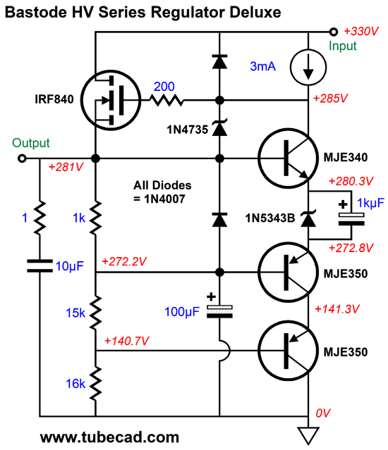
The added 1N4007 diodes and zener provide discharge paths at shutdown. The 1N4735B zener limits the maximum source-to-gate voltage to only 6.2V. In other words, if the output is accidentally shorted to ground, we do not want the MOSFET to try to deliver 30A; the zener limits the maximum current flow to about 3A. Of course, a fuse should be placed in series and it should blow before the MOSFET dies. The zener also limits the MJE340 NPN transistor's maximum base-to-collector voltage to 6.2V.
Patreon
More Series Regulators
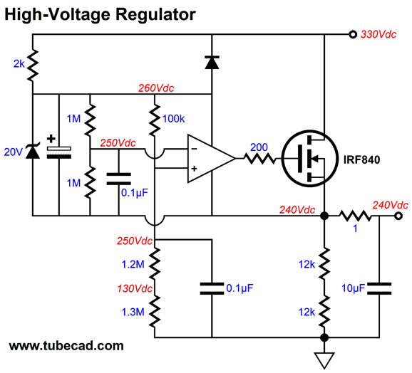
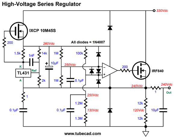
Missing from the schematic is the external 100mA load. Absent that load, the 2k resistor makes little sense. I choose this relatively low value to allow 240V regulation with raw B+ voltage of only 280Vdc. While this extends downward the range of raw B+ voltage, extending it upwards create excessive heat from the 2k resistor. For example, if the raw B+ voltage climbed to 460Vdc, then the resistor would see a 200V voltage drop and draw 100mA, which implies a 20W dissipation from the resistor. The workaround is to use a constant-current source instead of the resistor. My first choice was either the IXCP 10M45S or the IXCP 10M90S depletion-mode MOSFET. Once I had these parts in mind, the idea of replacing as well the zener with a TL431/LM431 shunt regulator IC also entered my mind. Combining them resulted in the following schematic.
I am not entirely sure that the 1nF capacitor is needed or that it couldn't be arranged differently, say by shunting the 14k resistor. The idea behind this design is that the TL431 adjusts the IXCP 10M45S's current conduction, allowing it to draw no more current than is necessary to power the TL431 and the OpAmp, say about 3- to 6mA. Here is a circuit that I meant to show in my last post.
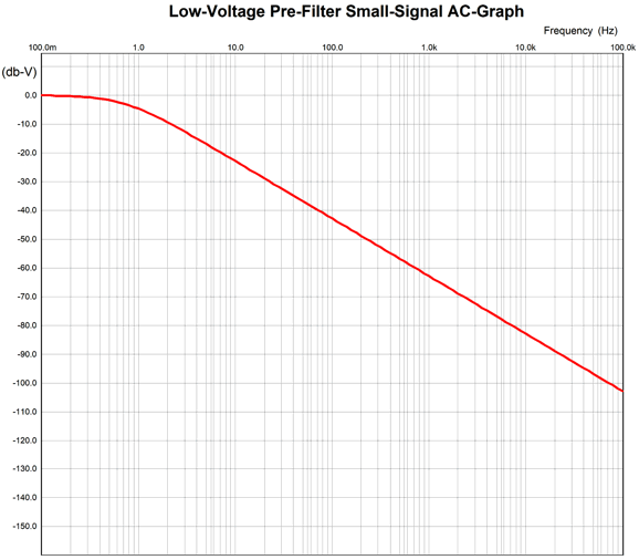
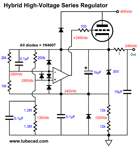
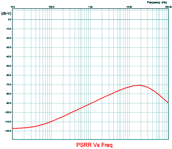
The OpAmp controls the Triode's output and sets the DC output voltage through the three-resistor string of 200k, 1.2M and 1.3M resistors. The OpAmp's 40-volt power supply is derived from the 30V zener diode and the through the triode and the two 12k resistors. Since the triode, say a 6AS7 or 12B4, offers just a small fraction of the transconductance of a high-voltage MOSFET, we need to be able to provide a huge span of potential grid voltage swing; thus, the 30V zener. The OpAmp should hold a FET input stage and be rated for at least +/-18V of power-supply rails voltages. The triode is a depletion-mode device, which means that can draw current with the grid negative relative to the cathode. I should mention that a good procedure to follow when building any OpAmp-filled high-voltage regulator is to start with a slow-OpAmp, as slow as the LM741, whose snail-like slew-rate of 0.5V/µs is far more likely to prove stable. If the slow OpAmp works, then move up to a slightly faster OpAmp—until you reach instability, forcing a retreat to the last stable OpAmp. In addition, the 0.1µF capacitor that spans from ground to the OpAmp's negative power-supply pin should actually be soldered to that pin. Not shown is the film or ceramic bypass capacitor shunting the OpAmp's power-supply pins—nonetheless, it is required. Here is the PSRR Vs frequency graph for this regulator.
The overwhelming majority of MOSFETs are enhancement-mode devices, which means that their gates must be positive relative to their source for them to conduct current. They do make, however, depletion-mode MOSFETs, which can draw a sizable amount of current with a negative gate voltage. In other words, we can replace the triode with a depletion-mode MOSFET.
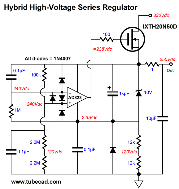
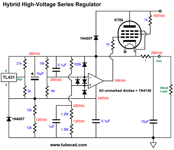
Since the MOSFET offer so much more transconductance than the triode, we do not need to deliver large gate-voltage swings. Thus, we can opt for a low-voltage OpAmp and lower-voltage zener (10V). The AD823 can work well within the 10V voltage envelope created by the zener and its output can almost swing to the rail voltages. In addition, due to its FET input stage, the input voltage can extend below the negative power-supply pin voltage. We take advantage of this feature by having the inverting input at the same voltage potential as the negative power-supply pin voltage through the 1M resistor. The 0.1µF capacitor attached to this input and resistor relays the AC signal at the positive power-supply pin, which tin turn attaches to the regulator output. In other words, the OpAmp will monitor the noise at the output and DC voltage at the bottom of the zener and compare the DC voltage to the DC voltage at its non-inverting input. The 100k and the two 2.2M resistors establish the output voltage, using the 10V zener as the voltage reference. The AD823 is a long-in-the-tooth OpAmp, which is obvious from its relatively high idle current draw. Today, they make low-current, low-voltage, rail-to-rail output, tiny surface-mount OpAmps that draw less than 1mA. The problem with many with of them is that they hold a transistor-based input stage rather than a FET-based input stage. The result is that their input impedances are about 300k, while the FET OpAmp delivers an input impedance of 300M. Let's return to hybrid high-voltage regulators that use a tube as the pass device. Here is a variation that uses a KT88 wired as a triode and uses a TL431 shunt-regulator/voltage-reference in place of a zener as the voltage reference.
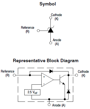
In post 31, the TL431 is the star of the show. Here is a quote from the post:
The TL431 holds and internal voltage reference and offers us an adjustment pin, which allows us to create an adjustable voltage reference that spans a voltage range of 2.5V to 36V. In other words, the TL431/LM431 can be configured as a fancy zener that offers far superior performance, with only two liabilities. The first is that it is dissipation limited due to its tiny size, being only 0.78W for the TO-92 package; the second is that we must avoid a range of shunting capacitances that create instability. Capacitors less than 3.3nF and more than 4.7µF are safe.
Okay, here is the high-voltage regulator.
The TL431 is configured as a 20V voltage reference. The OpAmp controls the KT88's cathode voltage by varying the KT88's grid voltage; thus, the ideal grid voltage would be at the center of the OpAmp's entire potential voltage swing; in this example, the center voltage is 250Vdc. Note that the regulator is under load (50mA externally). Unloaded, the KT88 sees a current flow of a tad over 10mA, and the grid voltage falls to 246Vdc; with a load of 100mA, the grid voltage climbs to 254.4V. Note that the KT 88's heater element must be floating and tied to the cathode; it can be either AC or DC voltage. As I looked over this circuit, I wondered if we could dispense with the OpAmp, as the TL431 held an internal amplifier. (In fact, the TL431 can be used as a single-ended audio-signal amplifier.)
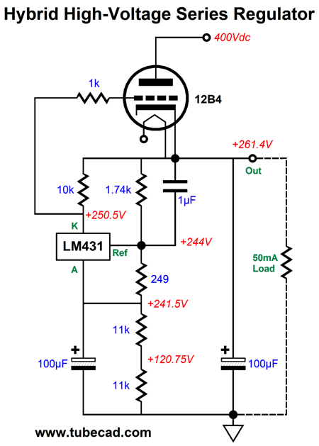
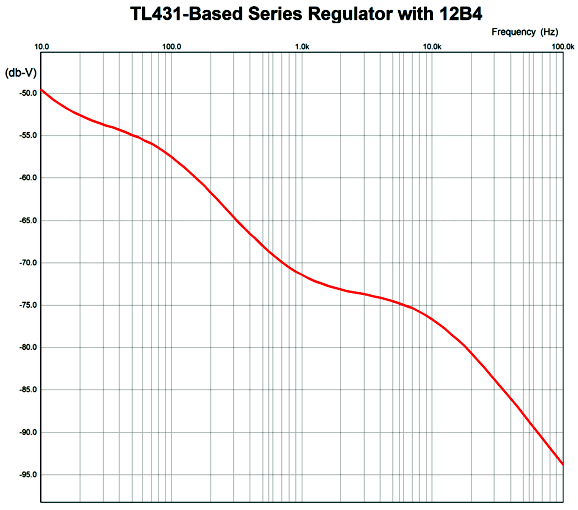
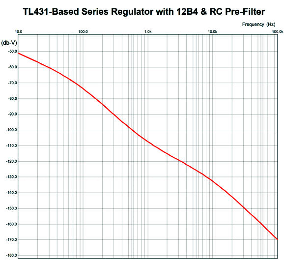
The TL431's internal voltage reference is used both to establish a fixed DC voltage of 20V for the TL431 to work within and to create a constant-current source of sorts. Its internal OpAmp controls the 12B4 pass device's current conduction. That is an amazing amount of tasks for a three-pin IC to perform. The TL431 strives to see a 2.5V voltage difference between its anode pin and its reference pin, which means that 249-ohm resistor sees a fixed 2.5V voltage drop, hence a constant-current draw of about 10mA. The TL431 draws about 1mA, which added to the 10mA yields a total of 11mA. The 11mA against the two 11k resistors in series creates a voltage drop of about 242Vdc, which we add 20V to get our output voltage of 262.8V. If we used two 10k resistors in series instead, the output voltage would fall to 246.3Vdc; with two 12k resistors, the output voltage climbs to 278.5Vdc. The 100µF capacitor that spans from ground to the TL431's anode provides the AC signal reference of ground, while the 1µF capacitor that bridges the reference pin to the output provides the AC error signal for the TL431 to react against. Here is the SPICE-generated PSRR graph for this simple high-voltage regulator. As we can see, the PSRR at 100Hz is -57dB. We can enhance the PSRR by placing an RC filter in front of the 12B4's plate, say a 100-ohm resistor and 100µF capacitor.
Note the huge improvement at 100kHz. In addition, a good move would be to replace the 10k load resistor with a 1mA constant-current source, such as the LM334, which would increase the part count by only one device, the LM334. Nonetheless, it is stunning that we can create a high-quality high-voltage series regulator with so few parts. Speaking of few parts, we can make a high-voltage regulator with an LM317-HV.
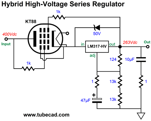
The KT88 forms a cascode with the LM317-HV, which has no idea that it is used in a high-voltage circuit, as the DC voltage window which in it works is only 5V to 50V big. The 50V zener protects the solid-state regulator from seeing too large a voltage drop; the LM317-HV's voltage limit is 57V. The voltage differential between its output and its adjustment pin is 1.25V, so the 124-ohm resistor sees a current flow of about 10mA, which against the 26k presented by the two 13k resistors in series creates a 260V voltage drop. We can get fancier still, as we can add two capacitors and two diodes.
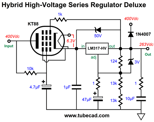
The KT88 is no longer triode-connected; instead, it operates as a pentode (actually, a tetrode; remember that the "KT" in "KT88" stands for kinkless tetrode). The 10k screen resistor and 4.7µF capacitor form an RC filter that delivers clean DC to the screen, which exercises a far greater control of current flow through the pentode than the plate. (In other words, this is a cheat or freebie of sorts, as the screen only draws a fraction of the current that the plate does, which means we get far better PSRR without having to pay for it with huge capacitors.) The additional 1µF capacitor forms an RC filter with the pentode, thereby pre-filtering the DC entering the solid-state regulator. The 3V zener and 1N4007 diode are there to protect the LM317-HV from damage at turn-on and turn-off.
Unanticipated Amplifiers Another lament grows in my mind and heart: the Annual RMAF Unanticipated Amplifier Challenge. This was a running joke of sorts with me and some amplifier designers, which I hinted at in previous posts. The idea was simple: design a solid-state power amplifier that a certain famous amplifier wizard could not imagine existing, as the only topology he seemingly could imagine is the standard three-stage effort of a differential input stage followed by common-emitter VAS driver stage and ending with either an emitter-follower or compound output stage.
Of course, his rebuttal would be that this conventional topology cannot be improved upon, much like four-wheel cars cannot be improved upon, which explains why we do not see three-wheel and five-wheel cars on the road. The actual name of the challenge bore a name that was a pun on this amplifier designer's last name, which I will not name. Why not? We did not seek to chastise or denigrate, but at most to gently chide, for he is indeed worthy of his master status. In other words, the challenge was to create a design entirely unanticipated and unimagined due to its departure from predictable practice. Okay, this may seem like an exercise in seeking novelty for the sake of novelty, which perhaps it mostly was. As I looked over my first entry from about six years ago, however, I marveled at the soundness and thoroughness of the design.
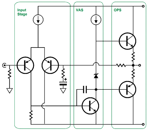
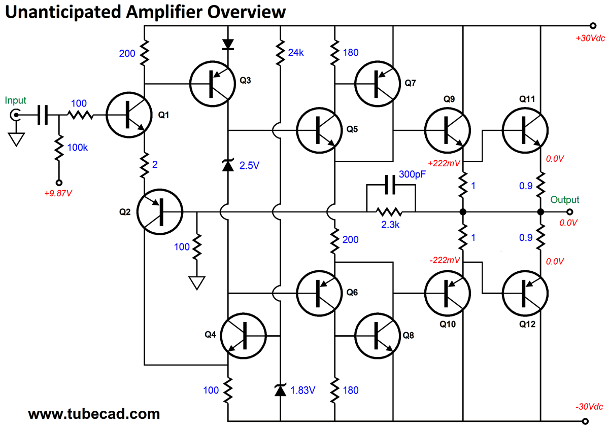
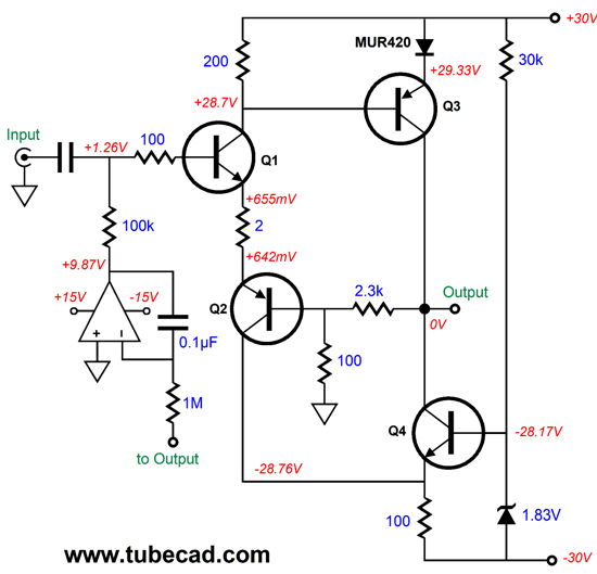
This is not your father's or your grandfather's solid-state power amplifier, as it has no progenitor and has my paw* prints all over it. The input stage is formed by transistors Q1 and Q2, which are arranged in a bastode topology. The bastode is a vertical differential amplifier that does not require a constant-current source or long-tail resistor; it does however, require dissimilar base voltages; thus, the input coupling capacitor and the bias voltage of 9.87V, which falls to 1.26V at the input transistor (Q1) base. The negative feedback input is Q2's base. Here is the input stage and driver stage isolated from the amplifier.
My assumption was that all four transistors must share the same idle current, so the 200- and 100-ohm resistor values would make sense, as both resistors would ideally see the same voltage drop, but the 100-ohm resistor would see twice the current flow. Well, in SPICE simulations, the lowest distortion obtained with the Q1 and Q2 drawing 6.5mA, while Q3 and Q4 drew 5.8mA. Transistor Q3 is configured as a common-emitter amplifier, while transistor Q4 is configured as a common-base amplifier. In other words, transistor Q3 gets its input signal from its base, while Q4 gets its signal from its emitter. The result is a push-pull operation. To see how this works, imagine a positive input signal to transistor Q1's base. The transistors Q1 and Q2 increase their current flow, which creates a larger voltage drop across the 200-ohm collector resistor, which in turn further increases Q3's conduction, pulling the output up. In contrast, Q4's conduction decreases, as the increased current flow through its 100-om emitter resistor creates a larger voltage drop, thereby reducing Q4's emitter-to-base voltage, causing Q4 to release some of its grip on the output voltage. If the input signal to Q1 goes negative, then Q3's current conduction falls, while Q4's rises. Push-pull in a nutshell. The MUR420 rectifier is there to provide a fixed voltage drop to transistor Q3's emitter, which will force the same voltage drop added to its base voltage, which allows us to use the 200-ohm collector resistor, rather than some smaller value. The larger collector resistor value is, the more gain we get from the input stage. The 2V zener voltage was specified to ensure an equal current draw at idle from both the input stage and the driver stage. The 100-ohm and 2.3k resistors form the negative feedback loop and set the gain to 1:24 (27.6dB), as (100 + 2300)/100 = 24. Note that the typical big-valued capacitor that usually terminates the 100-ohm feedback resistor is absent. Hallelujah! This capacitor is a damned nuisance. Why is it usually included? The quick answer is to reduce the DC offset voltage at the amplifier's output. The way it works is that it is effectively a dead short in AC terms, but an open circuit in DC terms. Thus, the amplifier delivers an AC gain set by the ratio between the two negative feedback resistors, but unity gain at DC voltages, which means substantially more negative feedback with DC. My terminating the 30k resistor into the positive power-supply rail voltage rather than ground is a subtlety. If the fuse on the positive power-supply rail opens, transistor Q4 loses its bias voltage and shuts off, as do Q1, Q2, and Q3. Thus, the output does not slam to the negative rail voltage; so, too, if the negative power-supply rail fuse opens. By the way, if this topology looks familiar, you have a dang good memory, as it appeared in post 398.
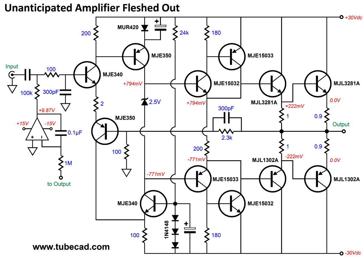
N- and P-channel FETs replace the transistors in the bastode input stage. A DC servo eliminates the DC offset from the output. In fact, this is how we develop the needed 9.78V to bias the input transistor.
Okay, let's return to the schematic and include the DC servo and the part values.
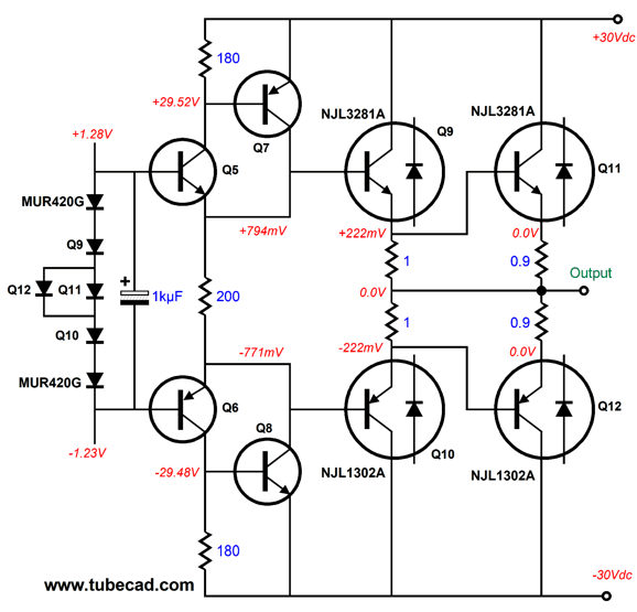
At the input, we see an added 300pF capacitor that limits RFI into the amplifier and improves high-frequency stability. The MJE340 and MJE350 are 20W, 300V transistors in the TO-225 package. The MJE15032 and MJE15033 are 50W, 250V transistors in the TO-220 package. The MJL1302A and MJL3281A are 200W, 260V transistors in the TO-264 package. In short, all the transistors are over-specified for their tasks. No TO-92 tiny transistors here. The 1.83V zener has been replaced by three 1N4148 diodes in series, which are bypassed by a large-valued capacitor, say 1kµF/6.3V. The MUR420G rectifier also gets a bypass capacitor. Now let's look at the output stage (OPS) in detail.
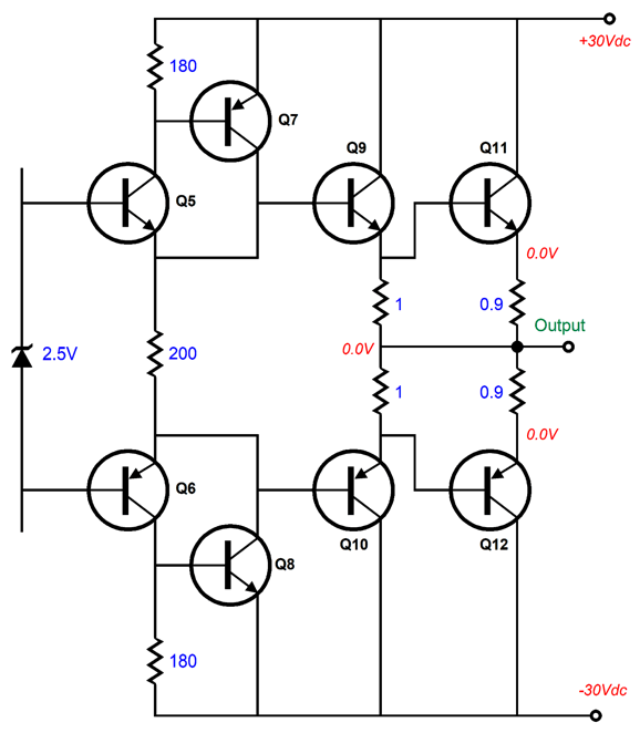
Transistors Q5 & Q7 and Q6 & Q8 form compound emitter followers stages, which offer lower output impedance and greater linearity over the conventional emitter-follower unity-gain buffer stage. In addition, they further unload the voltage-gain stage (VAS). At idle, output transistors Q9 & Q10 draw 223mA of current, while transistors Q11 & Q12 are completely tuned off. Yes, this is one of my anti-2gm efforts that strives to achieve a constant-transconductance output stage by wedding a class-AB stage to a class-C stage.
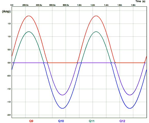
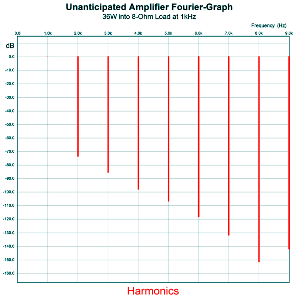
When transistors Q9 doubles in current conduction, transistors Q10 shuts off and transistors Q11 starts to conduct. The output impedance remains the same as it was at idle and amplifier behaves as if it were running a class-A OPS. Here is the SPICE-generated graph for 36W of output into an 8-ohm load at 1kHz. The four plotlines show the four output transistor current conductions.
We can see that the transitions from on and off line up well, which is reflected in the Fourier graph of the harmonics.
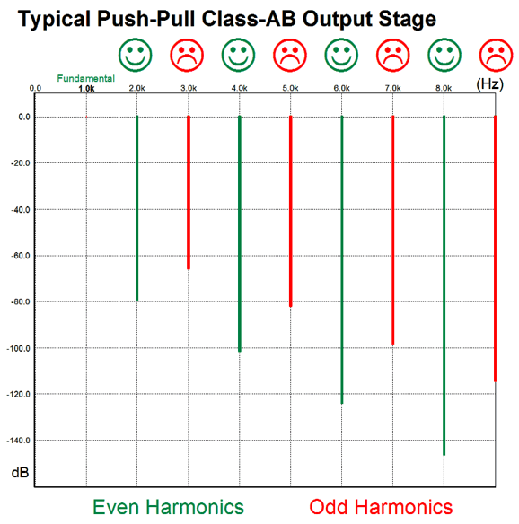
Dang single-ended, class-A looking isn't it? The THD is 0.022% but that is not as important as the harmonic structure. Let's compare this to the conventional solid-state class-B power amplifier's harmonic structure.
I know why so many instantly fell in love with single-ended power amplifiers, as they do not exhibit this typical harmonic structure, which quickly fatigues our ears and soul. The huge problem, of course, is that we cannot get 36W of single-ended power from one 300B or one 845. Now, the theoretical maximum efficiency of a class-A output stage, whether single-ended or push-pull, is 50%, but actual tube-based single-ended output stages are closer to 25% to 33% efficient, so 36W implies something like 100W of dissipation at idle, whereas this solid-state amplifier dissipates only 14.7W total at idle. Moreover, the cost of all the parts are less than one new-production 300B. (Actually, the most expensive parts are the heatsink and enclosure.) The conventional class-B emitter-follower output stage can deliver amazingly good results under optimal conditions. The huge problem is that these conditions are a moving target. For example, the theoretical perfect bias current of 118mA can be achieved on a test-bench with some fiddling. But actual amplifier use in a home with music playing introduces problems. The most important of which is that the output transistors are very temperature dependent, as the emitter-to-base voltage changes with temperature.
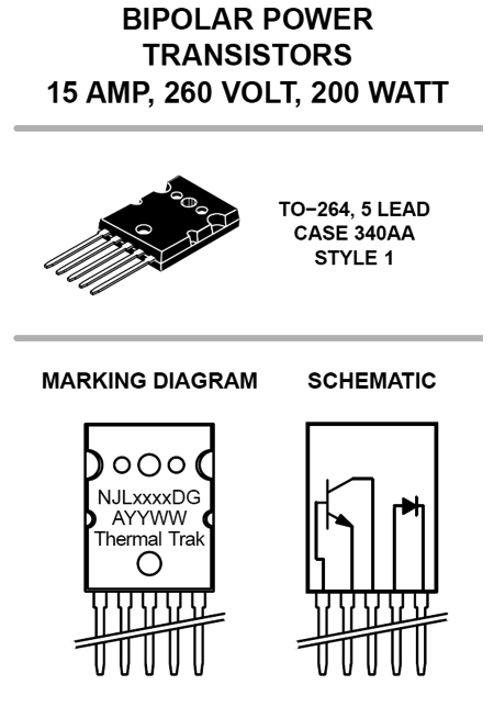
As the heat rises, the emitter-to-base voltage falls, which throws the bias current off as the transistor conducts far more current. Well, doesn't the automatic biasing compensation circuit kick in and correct the problem? It does—after some time passes. The transistor's junction temperature rises instantly, but its case temperature lags a bit, then the heatsink slowly climbs in temperature. If the truth be told, the real purpose of this bias circuit is not to achieve low crossover distortion, but to prevent thermal runaway. One ingenious workaround is to place a diode within the transistor package, so less of a thermal lag time occurs when reading the voltage drop across this diode compared to the external diode attached to the heatsink. This is what some Sanken transistors and the On Semiconductor ThermalTrak™ NJL1302D and NJL3281D output transistors do.
In a class-B emitter-follower OPS with optimal bias current (118mA) and optimal emitter resistor values (0.22 ohms), the voltage drop across the resistors is only 26mV; in contrast, the voltage across my class-AB+C primary emitter resistors is 223mV, almost nine times greater, so its sensitivity to emitter-to-base voltage shifts is almost nine times less. This is an excellent starting point. Next, we use the On Semiconductor ThermalTrak™ NJL1302D and NJL3281D output transistors to create a thermally-tracking voltage reference for the output stage.
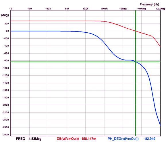
Two MUR420G rectifier diodes are added to the diode string. In SPICE simulations, the thermal tracking was impressive. The key point is that transistors Q11 & Q12 only turn on when Q9 & Q10 double in current flow. Thus, we want all of transistors Q9 & Q10 bias-voltage shifts and only half of transistors Q11 & Q12 voltage shifts included in the reference voltage total. This is a subtlety, but it makes sense if you think about it. Okay, what about the amplifier's frequency response and phase response? The frequency where the output gain falls to unity is critical, as we need to see plenty of phase margin.
The -3dB frequency is 160kHz. The phase shift at 20kHz is only -6 degrees. In summary, I was going to create a new Unanticipated Amplifier for this post, so I sought to review my previous efforts, but the first design gripped me. What had started as something of a gag design proved far more interesting. If the RMAF still survived, this design would have languished on my hard drive, unlikely to ever be seen again. Of course, we could build a far more powerful version by simply increasing the power-supply rail voltages and duplicating transistors Q9 through Q12 three times, so something closer to 200W was obtainable. Imagine hearing 200W of single-ended-quality sound!
Music Recommendation: Dinosaur's To The Earth I played a joke on myself, as I thought the recording was a 16-bit, 44.1kHz, CD-quality effort. It wasn't. It was 24-bit and 96kHz. My mistake and my delight in being mistaken. (As I listened to the high-res recording, I thought, "Damn, this sounds great; I do not unstand how CD quality can sound so fine." I have given it three listens so far, and I like more each time. I know that is is available on Amazon Music streaming music service.
//JRB
*Paw of the Lion, La Griffe du Lion
User Guides for GlassWare Software
For those of you who still have old computers running Windows XP (32-bit) or any other Windows 32-bit OS, I have setup the download availability of my old old standards: Tube CAD, SE Amp CAD, and Audio Gadgets. The downloads are at the GlassWare-Yahoo store and the price is only $9.95 for each program. http://glass-ware.stores.yahoo.net/adsoffromgla.html So many have asked that I had to do it. WARNING: THESE THREE PROGRAMS WILL NOT RUN UNDER VISTA 64-Bit or WINDOWS 7, 8, and 10 if the OS is not 32-bit or if the OS is 64-bit. I do plan on remaking all of these programs into 64-bit versions, but it will be a huge ordeal, as programming requires vast chunks of noise-free time, something very rare with children running about. Ideally, I would love to come out with versions that run on iPads and Android-OS tablets.
|
I know that some readers wish to avoid Patreon, so here is a PayPal donate button instead. Thanks. John Broskie
John Gives
Special Thanks to the Special 89
I am truly stunned and appreciative of their support. In addition I want to thank the following patrons:
All of your support makes a big difference. I would love to arrive at the point where creating my posts was my top priority of the day, not something that I have to steal time from other obligations to do. The more support I get, the higher up these posts move up in deserving attention.
If you have been reading my posts, you know that my lifetime goal is reaching post number one thousand. I have 447 more to go. My second goal is to gather 100 patrons. I have 16 patrons to go. Help me get there.
Only $9.95
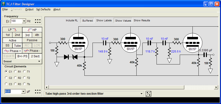
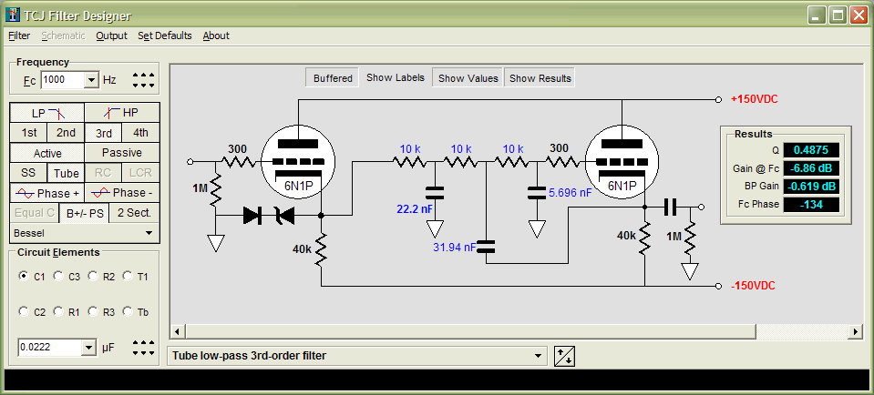
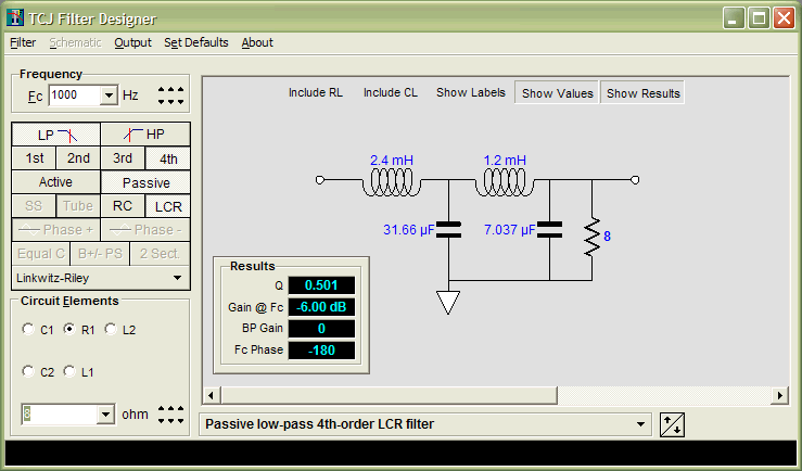
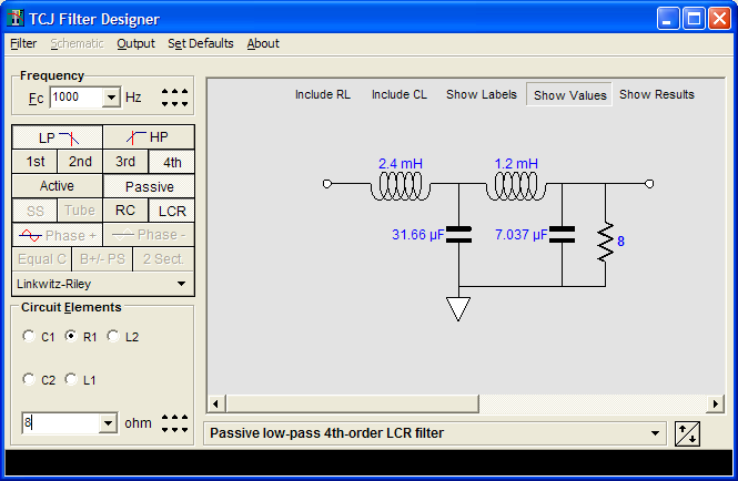
The Tube CAD Journal's first companion program, TCJ Filter Design lets you design a filter or crossover (passive, OpAmp or tube) without having to check out thick textbooks from the library and without having to breakout the scientific calculator. This program's goal is to provide a quick and easy display not only of the frequency response, but also of the resistor and capacitor values for a passive and active filters and crossovers. TCJ Filter Design is easy to use, but not lightweight, holding over 60 different filter topologies and up to four filter alignments: While the program's main concern is active filters, solid-state and tube, it also does passive filters. In fact, it can be used to calculate passive crossovers for use with speakers by entering 8 ohms as the terminating resistance. Click on the image below to see the full screen capture.
Tube crossovers are a major part of this program; both buffered and un-buffered tube based filters along with mono-polar and bipolar power supply topologies are covered. Available on a CD-ROM and a downloadable version (4 Megabytes). Download or CD ROM
|
|||


| www.tubecad.com Copyright © 1999-2021 GlassWare All Rights Reserved |