| John Broskie's Guide to Tube Circuit Analysis & Design |
|
10 October 2019 Post 479
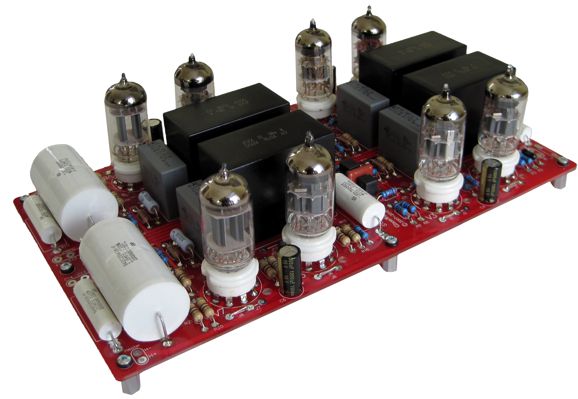
Aikido PH-2 and Tube Rectifier
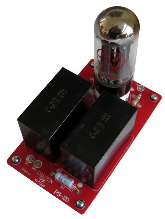
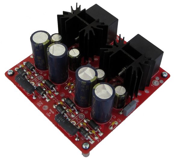
My answer was that he could simply place the two heater strings in the PH-2 in parallel and use the Janus' single heater regulator to power all eight heater elements. Now, I have a better idea: use a PS-20 and a Dual/Bipolar LV-Reg.
The PS-20 is a super simple high-voltage power supply that uses a tube rectifier and two polypropylene capacitors in its RC filter to create the B+ voltage. (I would replace the RC resistor with a choke.) The Dual/Bipolar LV-Reg holds two separate heater regulators.
With these two power-supply PCBs, you can run the tube rectifier and an electrolytic-capacitor-free B+ voltage. This could make a killer setup. here is why: if you take the power transformer's 6.3Vac winding and rectify it, you will see inverted spikes in the high-voltage secondary's AC waveform due to the huge but brief current surges through the low-voltage winding as it charges up the huge-valued capacitors needed for the heaters. I believe this is why some prefer to run AC on the heaters; it makes the B+ smoother. Now, if we use a separate toroid for just the two heater regulators and a conventional tube power transformer for the B+ voltage, taping up its 6.3Vac winding, we get the best of both worlds: separate DC regulators for the heaters and tube-rectified B+ voltage. The only thing missing is one of my Switch-AC assemblies.
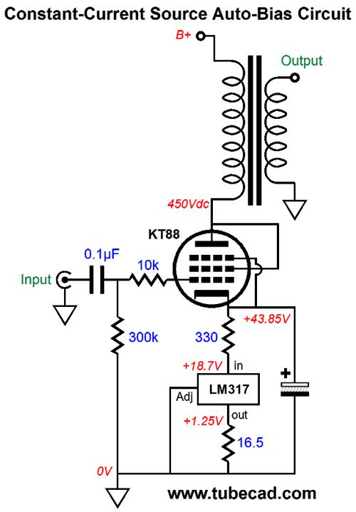
More Adventures in Class-A In passing in my last post, I mentioned my constant-power class-A designs, which strive to maintain a fixed heat dissipation, regardless of the variations in wall voltage. Most of my design examples were solid-state efforts, with the exception being a few tube-based single-ended designs in post 349. But before we examine constant-power circuits, let's look at the easiest way to auto-bias a single output tube in a single-ended amplifier.
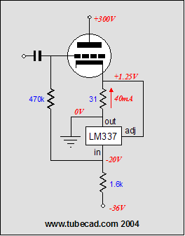
The LM317, a linear adjustable voltage regulator, has been configured as a constant-current source. We set the desired idle current by varying the LM317's output resistor's value. The math is super simple: Iq = 1.25V/resistance. In the example shown above, we get about 76mA with the 16.5-ohm resistor. The added 330-ohm resistor is there to limit both the LM317's dissipation and voltage drop, as the LM317 is only rated for 37V; on the other hand, we can use an LM317-HV, which can withstand 57V. This circuit works well, but it is indifferent to the variations in wall voltage.
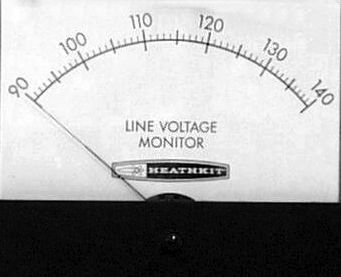
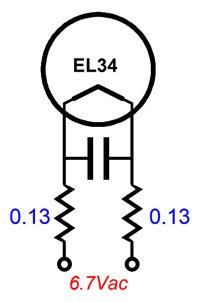
In the USA, the wall voltage standard is 117Vac, but I have lived with 115Vac to 122Vac. In general, wall voltages have climbed over the decades, starting with 105Vac, 110Vac, 112Vac, and then 115Vac. In fact, most old power transformers for tube applications are rated for a 115Vac wall voltage. So what happens if we hook up a 115Vac primary to 122Vac? We get more secondary voltage. How much more? Divide 122Vac by 115Vac and we get 1.06, which means that if the B+ voltage was once 500Vdc, it will now be 530Vdc. In general, this is not that big a deal for most tubes in most class-AB power amplifiers, but it can be a problem in class-A tube-based amplifiers, as we must run the output tubes extra hot, usually near the hairy end of their dissipation limits. In addition, tube heater elements suffer, as rather than the expected 6.3Vac they see 6.7Vac, which will shorten the tube's life span. My workaround has been to place two series resistors on each side of the heater element. For example, with an EL34, I place two 0.13-ohm resistors to drop the AC voltage down to 6.3Vac. In addition, I shunt the heater element with a 0.1µF ceramic capacitor. Of course, if the power transformer was rated for an input voltage of 112Vac, larger-valued resistors will be needed.
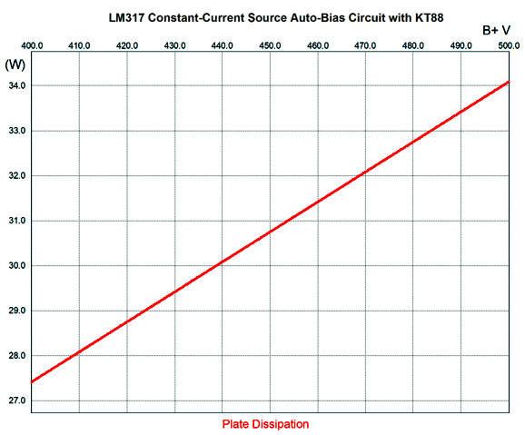
Let's look at the change in plate dissipation with a varying B+ voltage, when we hold the idle current steady.
Note the straight line, which makes sense, as the current was fixed by the constant-current source, while the B+ voltage varied. Getting to a constant-power plate dissipation at idle requires something fancier. First of all, we must switch to grid bias, as the cathode bias setup does not lend itself to constant power without wasting a lot of power. (A possible exception might be some of my LM337-based auto-bias circuit designs.)
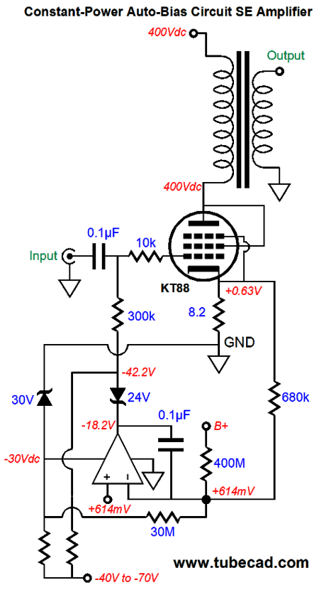
Okay, here is one solution.
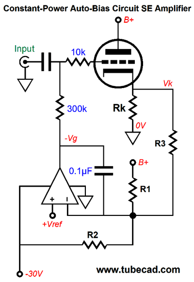
The OpAmp runs off the -30V power-supply rail voltage and ground. Most OpAmp can withstand a 30V power supply differential, with some, like the LF442 and LF444, working up to 40V of power-supply voltage differential. Not all OpAmps, however, can tolerate input voltage more positive than their positive power-supply voltage. In general, FET input stages work best here. The procedure is easy enough: we find R1's value by multiplying the B+ voltage by 1Meg. For example, with a B+ voltage of 400V, we would use a 400M resistor for R1. True enough, they don't make a 400M resistor; even if they did, we would not want to use it, as the 400V would likely exceed the resistor's maximum voltage differential. This maximum is different from its maximum heat dissipation. In fact, even with the 400 volt voltage drop, the 400M resistor will dissipate only 0.4mW. Not much at all, but its 300V or 350V maximum voltage drop will be exceeded. The workaround is to place four 100M resistors in series. We find R2's value by multiplying the OpAmp's negative power-supply voltage by 1Meg. In this example, with a voltage of 30V, we would use a 30M resistor for R2. This leaves finding R3's value. Alas, here some experimentation is needed, either in reality or with SPICE. A starting guess value for R3 is the reference voltage against 1Meg. Looking at the schematic, it looks like the voltage and resistor relationships might be something like: R3 = (1 + 30V/400V)*Vref*1M. In this example Vref is 0.614V, which is the voltage drop of a 1N4007 with two 200K resistor in series with it and a 400V voltage drop across the entire string. After some fiddling in SPICE, here is the value for R3 I found.
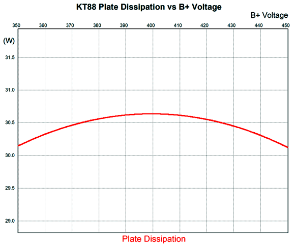
The 680k worked well enough to produce the following graph.
A spread of 100V in B+ voltage only resulted in a 0.5W shift in plate dissipation. Note the 24V Zener, whose purpose is to extend the OpAmp's negative voltage swing to below its negative power-supply rail voltage. At idle, the OpAmp's output should sit at roughly half of its negative power-supply rail voltage, as that would allow the greatest range of adjustment from the OpAmp. In other words, with different output tubes, a higher-voltage zener might be needed, for example with 300B output tube, or, perhaps, no Zener might be needed, for example with an EL84 output tube. The secret behind this circuit's workings is the fixed voltage provided by the 30V Zener. We use this 30V reference voltage to create a faux constant-current source out of the 30M resistor. A fixed voltage drop across a fixed resistance equals a constant-current draw. In other words, we could replace the 30M resistor with a 0.001mA constant-current source. If we wanted to get extra fancy, we could shunt the 8.2-ohm cathode resistor with two 1N4007 diodes in series and forward biased, so if the KT88 is forced beyond its class-A peak current limit (154mA), the DC servo's 0.1µF capacitor will not become over charged, which would end up lowering the idle current until the capacitor discharged sufficiently.
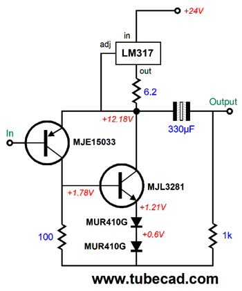
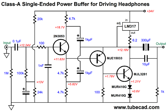
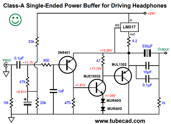
Class-A Single-Ended Power Buffer for Driving Headphones
The LM317 is put to use as a constant-current source and the PNP MJE15033 and NPN MJL3281 are configured in a compound arrangement, wherein the PNP transistor controls the NPN transistor. The two diode in series are there to allow a larger-valued collector resistor value for the MJE15033 PNP transistor
I feared that the PNP transistor's input impedance would prove too low for wimpy tube line-stage amplifiers, so I decided to place an emitter follower in front of it.
The 2N3053 is a fun little NPN transistor that comes in a metal can (TO-39) and offers a high current gain. The two 1kµF capacitors serve as bootstrap capacitors that both shield the 2N3053 from the power-supply noise and allow the transistor to swing much larger output voltages. In SPICE simulation, the circuit performed quite well.
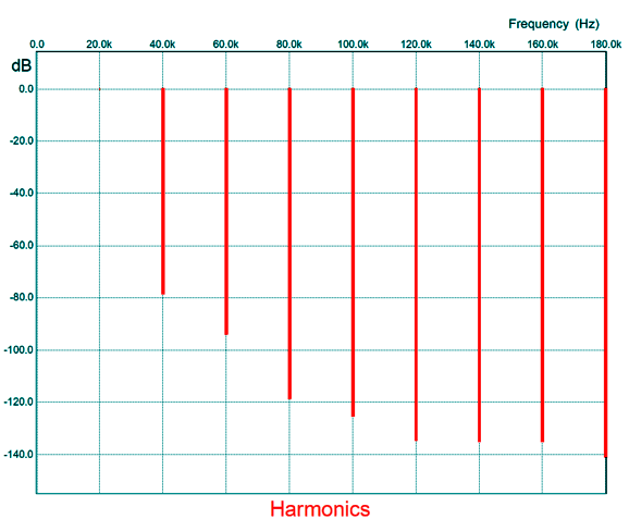
Note that this Fourier graph is based on the output of 4Vpk into a 50-ohm load at 20kHz. Not bad at all. Yet, this circuit didn't suit me, as I wondered if I couldn't make better use of three transistors and a constant-current source. The snag appeared to be the input 2N3053, which worked as a buffer to drive the output buffer, but offered no negative feedback to the output signal. I decided to try a PNP transistor instead.
The 2N5401 PNP input transistor monitors the output signal at its emitter and compares that signal to the signal at its base, relaying the adjustment signal to its collector and, in turn, the NPN MJE15032's base, which then drives the PNP MJL1302. The results were gratifying.
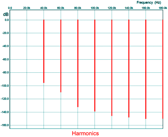
Note the reduction in all the harmonics. The maximum peak voltage swing into the headphones is equal to the idle current against the headphone impedance. For example, with the 200mA idle current and with 40-ohm headphones, we get 8Vpk. If higher idle current draw is needed, I would place another LM317 and current-setting resistor in parallel the existing LM317. Why? The obvious answer is less heat dissipation per device, but in addition the LM317 is not an LDO (low drop out) voltage regulator and the required minimum input-to-output voltage differential increases with higher current flow.
Single-Ended / Push-Pull Power Buffer
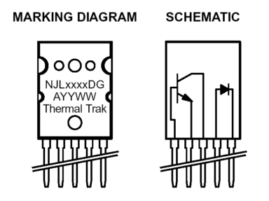
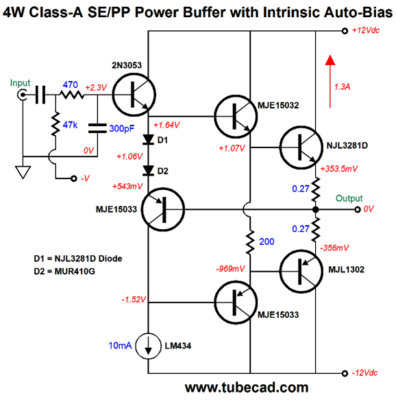
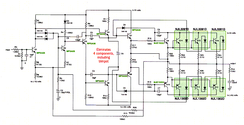
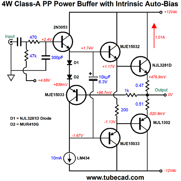
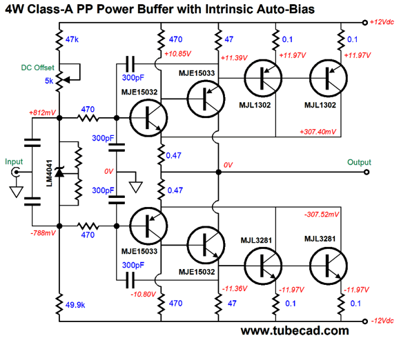
When I first encountered the interesting five-pin output transistors from ON Semiconductor (formally Motorola) that held an internal diode, I poured over the data-sheet, hoping to find some clever new uses for the NJL1302D and NJL3281D. Alas, the voltage drop across the diode didn't exactly match the transistor's own base-to-emitter voltage differential, but it did track the transistor's change base-to-emitter voltage in relatively real time. The diode is electrically separate from the transistor but rests on the same substrate, so the thermal time lag is tiny, particularly when compared to the conventional tracking of the heatsink temperature. Bob Cordell found that the diode voltage drop reduced by -1.7mV per C ° increase in temperature, while the transistor base-to-emitter voltage dropped by -2.1mV per C °. Then my interest was piqued again, when John Atwood gave me a handful of these ON Semiconductors. Once again I poured over the data-sheets and the example circuits they showed seemed even more flawed upon second viewing. I decided I would have to devise my own circuits. One circuit I came up made use of only one NPN NJL3281D transistor and used a plain PNP MJL1303 output transistor.
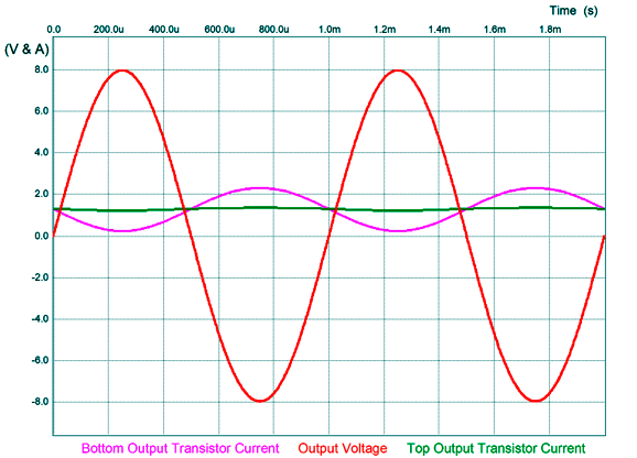
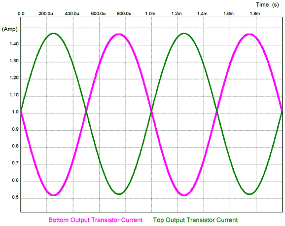
This is not your father's output stage. I designed this circuit when I was obsessed with mix-mode output stages, such as SE/PP and class-A/class-AB. First of all, it looks like a push-pull output stage, but it isn't. Well, at least not within the confines of its idle current flow. In other words, as long as the peak output current swing is less than the idle current, the output stage runs as a single-ended affair, with the top NPN output transistor behaving as a constant-current source. That's right: the top output transistor functions as a constant-current source.
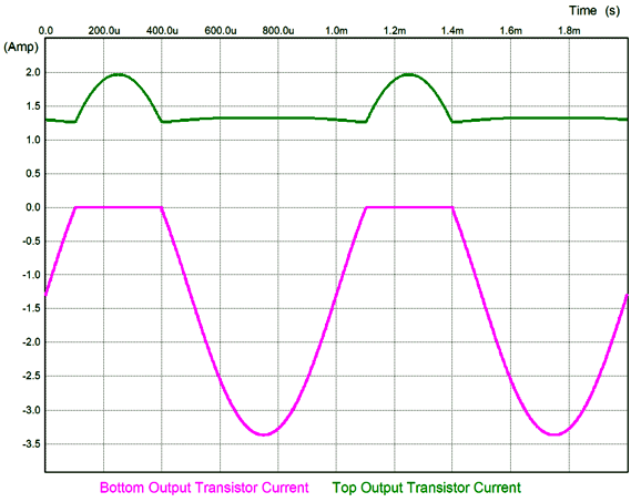
Note the NPN NJL3281D transistor (green plot line) is near flat, in spite of full output into an 8-ohm load. In contrast, the PNP MJL1303 output transistor swings up over 2A and down to almost zero amperes. If we force more output current beyond the idle current, however, then the top transistor increases its conduction and push-pull operation takes over. For example, with a 4-ohm load, we get the following results.
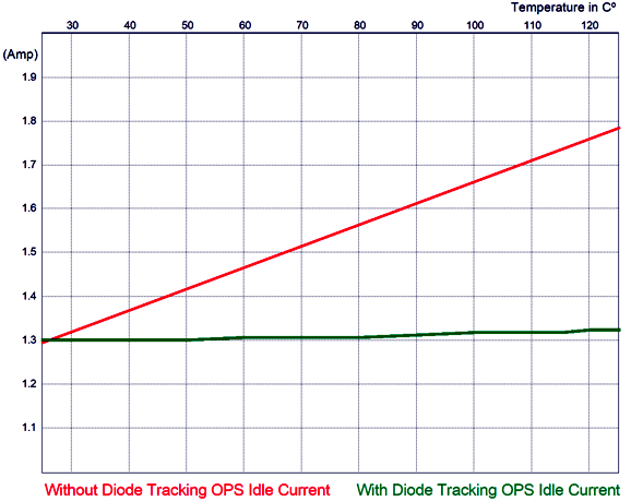
I filled the phase on the bottom transistor's current meter in SPICE< so we could better see the push-pull action. The top transistor's current flow, however, never falls below its idle current value. In contrast, the bottom output transistor experiences the big current swings, from zero to twice the idle current. Second, this output stage holds an auto-bias (with a temperature-compensation) feature due to the use of the NJL3281D and its internal diode, D1 in the schematic. Diode D2 is just an external two-lead MUR410G rectifier. As the NJL3281D transistor gets hot, so does its internal diode and both experience a roughly equal drop in voltage. In SPICE simulations, I varied both transistor and diode temperatures in 5C ° increments from 25C ° to 100C ° and I saw near perfect tracking.
Without the diode compensation, the idle current climbs steadily with increased temperature in a perfectly linear fashion, but the dissipation never hit my back-of-the-envelope calculations which put the 125 ° heated transistor idle current to over 2A. With the diode tracking, the idle current ever so gently rises a wee bit with increased heat—ruler flat would be ideal, this is close enough to what we want compared to steep upward sloping plot-line to meltdown. I was stunned by the results, as I know that others had not gotten similar results with the ThermalTrack™ transistors.
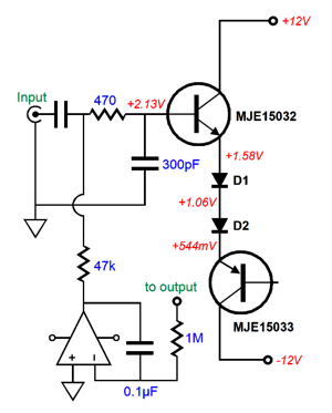
Based on the data-sheet, I was sure this setup would not work, as the data-sheet design example showed three internal diodes in series, not just one. In other words, I was sure that the single diode's voltage drop with increased temperature would prove too small. What might have made it work, however, might have been due to either the output stage running a class-A high idle current flow or the 10mA of current flow through the diode put it in its sweet spot. I know that Sanken power transistors with internal diodes specify an optimal diode current. (By the way, the Sanken transistors do not electrically separate the temperature-compensation diode from the transistor, which does improve the thermal tracking, but complicates using the diode, as it attaches to the transistor's base.) Adding a DC servo circuit to prevent offset voltages at the output would be easy, as the +/-12Vdc power-supply rail voltages are ideal for OpAmp use. (Please ignore the MJE15032, which should be a 2N3053.)
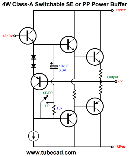
The only potential danger is making the input resistor too high in value, say 100k and up, as insufficient current would flow through the resistor to pull up the output voltage to 0Vdc. In other words, the OpAmp's output might swing up to it positive limit, yet the output stage might center at a negative voltage. One workaround is to replace the input NPN transistor (originally, an MJE15032) with a transistor with a higher beta, the 2N3053. (I came up with the topology over a decade ago, when I didn't know about how nice was the 2N3053, a transistor that a reader suggested to me.) The 2N3053 improved the performance, so it stays. Now things get even more interesting: with the addition of a large-valued capacitor, we can force the output stage to operate in class-A push-pull throughout.
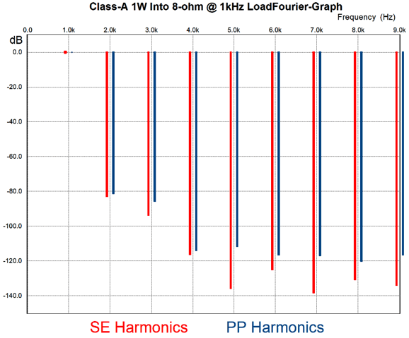
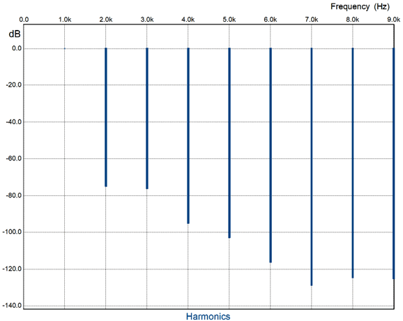
Now both output transistors push and pull, which means that we can halve the idle current and still remain within the class-A window of current flow. (If you plan on always running in push-pull mode, then place a 1k resistor in series with the output and the top MJE15033 base. How do these two arrangements compare? Here is the Fourier graph for 1W output into an 8-ohm load. Bear in mind, these graphs were generated with the old input transistor, the MJE15032; in contrast, the 2N3053 results in a less ragged higher harmonics. Still, the contrast between single-ended and push-pull modes remains evident with either input transistor.
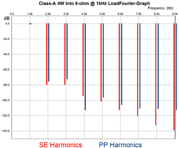
Note how the single-ended plots are all lower than the push-pull plot-lines. Now, look at the SE 5th and 7th harmonics, where we see the preternaturally deeper odd harmonic percentages. The only difference was the addition of the capacitor and the same idle current was used. Now, let's look at full output, in other words, 4W, or 8Vpk into 8 ohms.
The only harmonic that the push-pull version wins at is the 4th. We can even add a switch, so we can select between single-ended and push-pull operation. I would add an additional series resistor to the large-valued capacitor to keep it charged to prevent nasty spikes when flipping the switch as the amplifier is running, which we should never do but we often end up doing anyway.
I was going to leave this circuit here, but I decided to go all out and see what a purposely push-pull version would look like and how it performed.
I used larger emitter resistor values to lower the idle current. In addition, I got better balance with a larger resistor value for the PNP output transistor. Here is the what SPICE showed.
And here is the Fourier graph for 8Vpk at 1kHz into 8 ohms.
This topology could be scaled down, not so much in power-supply rail voltages, but in idle current draw, so that it could power headphones instead of loudspeakers. With an idle current of 250mA, we could get 8Vpk voltage swings into a 32-ohm load and still remain in single-ended mode.
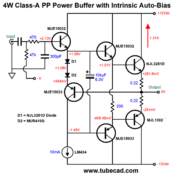
Class-A with Compound Output Stages
Once again, this is a power buffer that delivers current gain, not voltage gain. Tubes are happy to develop signal gain, but balk at delivering high current.
By the way, I have built "naked" tube-based single-ended output stages that held only output tubes, power supply, and output transformer, but no input or driver stages. These "naked" amplifiers required a hot tube-based line-stage amplifier to deliver the needed 30Vpk input signal for full output. These efforts were well received by listeners—more so than when the same line-stage amplifier circuit was contained in the power amplifier. A paradox. This puzzled me and I sought an explanation. One possibility was that the external line-stage amplifier held a high-voltage regulator, but the complete amplifier version didn't. Another possibility was that the interconnect cables sound better with the big voltage swings. Or, perhaps, the line-stage amplifier tubes didn't get rattled by the power amplifier's buzzing power transformer or stray electric fields. Okay back to the class-A solid-state power buffer with a compound output stage, note that the input transistors pass their collector signal to emitter followers that drive the output transistors. This arrangement allows us to use larger valued collector resistors, thus creating higher open-loop gain. Each output transistor gets its own 0.1-ohm emitter resistor, which prevents current hogging. The +/-12Vdc power-supply rail voltages limit the maximum output voltages swing to about 8Vpk, which translates into 4W into 8-ohm loudspeakers. With higher rail voltages and more output transistors, we could get far more output power. For example, with +/-30Vdc power-supply rails and eight output transistors and an idle current of 1.6A for push-pull class-A output, we could get 24Vpk and 3Apk and 36W of power output into 8-ohm loudspeakers. Each output transistor must idle at 0.4A and dissipate 12W at idle. In other words, big heatsinks and a big power transformer will be required—and a hot line-stage amplifier capable of delivering 24Vpk output voltage swings. Assuming that the line-stage amplifier will be located far from the power buffer(s), we face the problem of long interconnect runs of cable, which means potentially high capacitance. Driving high capacitance at big voltage swings and high-frequencies requires current. In other words, a 12AX7-based line-stage amplifier won't cut it. Even a 12AU7-based line-stage amplifier might stall, if it cannot deliver enough current. Remember, slewrate equals current against capacitance.
Music Recommendation: Inlakesh's The Gathering Check out this YouTube video to get a taste of what the CD is like.
Mind you, if your smart phone or tablet or computer doesn't sport massive subwoofers, you simply will not get the full impact. Alas, Tidal does not offer this album, but it does offer a few of Inlakesh's other albums, Didjeridoo Meditation and Medicine Work.
I had to buy their The Gathering CD, as it was just too fun and makes a great demo CD—besides, it might lead to some spiritual uplift. //JRB
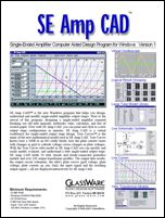
User Guides for GlassWare Software
For those of you who still have old computers running Windows XP (32-bit) or any other Windows 32-bit OS, I have setup the download availability of my old old standards: Tube CAD, SE Amp CAD, and Audio Gadgets. The downloads are at the GlassWare-Yahoo store and the price is only $9.95 for each program. http://glass-ware.stores.yahoo.net/adsoffromgla.html So many have asked that I had to do it. WARNING: THESE THREE PROGRAMS WILL NOT RUN UNDER VISTA 64-Bit or WINDOWS 7 & 8 or any other 64-bit OS. I do plan on remaking all of these programs into 64-bit versions, but it will be a huge ordeal, as programming requires vast chunks of noise-free time, something very rare with children running about. Ideally, I would love to come out with versions that run on iPads and Android-OS tablets.
//JRB
|
|
John Gives
Special Thanks to the Special 84 To all my patrons, all 84 of them, thank you all again. I want to especially thank
I am truly stunned and appreciative of their support. In addition I want to thank the following patrons:
All of your support makes a big difference. I would love to arrive at the point where creating my posts was my top priority of the day, not something that I have to steal time from other obligations to do. The more support I get, the higher up these posts move up in deserving attention. Only those who have produced a technical white paper or written an article on electronics know just how much time and effort is required to produce one of my posts, as novel circuits must be created, SPICE simulations must be run, schematics must be drawn, and thousands of words must be written. If you have been reading my posts, you know that my lifetime goal is reaching post 1,000. I have 524 more to go. My second goal is to gather 1,000 patrons. I have 917 patrons to go. Help me get there.
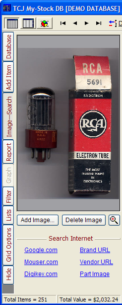
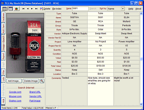
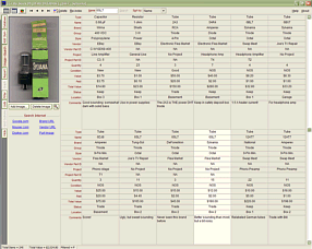
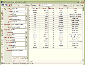
Only $12.95 TCJ My-Stock DB
Version 2 Improvements *User definable Download for www.glass-ware.com |
||


| www.tubecad.com Copyright © 1999-2019 GlassWare All Rights Reserved |