| John Broskie's Guide to Tube Circuit Analysis & Design |
30 December 2006
OTL amplifier design revisited
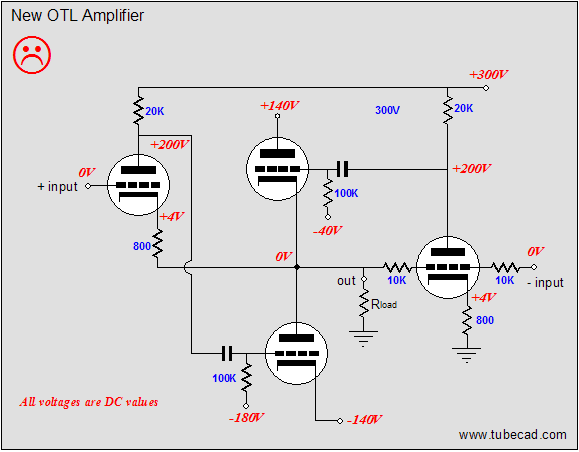
In redrawing the schematic, however, I realized that topology was just too big a jump for many, and that I needed to work my way up to this schematic in stages, starting with the underlying OTL topology without the crossover-notch-eliminating aspects of the circuitry. At the same time, I also realized that the schematic was too simple, that I had left out too many subtle, but important features for actual construction. So, let’s start anew. Below is the new OTL topology in its simplest terms.
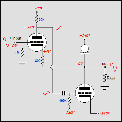
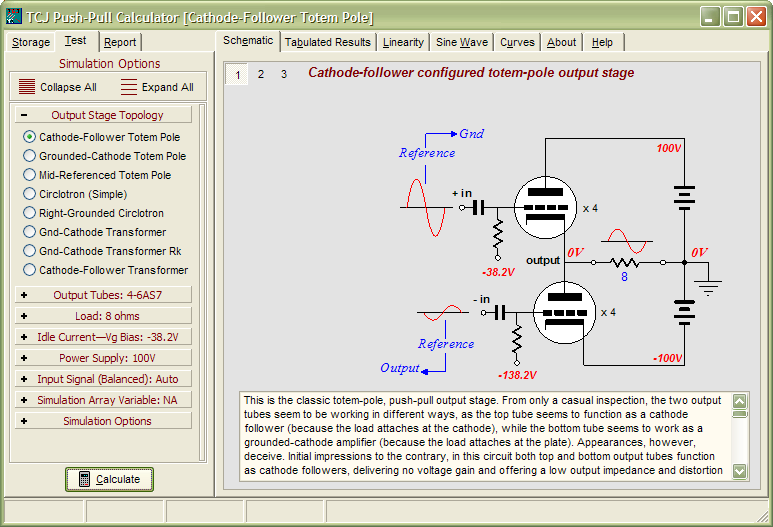
At its core are two output tubes in a totem pole, push-pull configuration. Flanking the two tubes are two driver tubes. The driver tubes accept a balanced input signal and then control their designated output tubes’ contribution to the output signal, working to keep the amplifier's output in line with the balanced input signal. As I look at it, this circuit reminds me of some of my takeoffs on the Murray amplifier. The idea behind the output-stage is that the two input tubes will each control its own output tube, by applying a feedback loop around the device’s output. At the same time, the imposed positive pulse would be greatly amplified by the rightmost triode, which relays the anti-phase amplified pulse to the top output tube’s grid. The top output tube then greatly decreases its conduction, thereby pushing the amplifier’s output negative. Why the sad face? As drawn, this circuit needs some help. But before moving on, let's make sure everyone gets the underlying idea here: that the output-stage strives for unity gain and that each output tube has its own feedback mechanism to correct any deviations from the input signal it sees. So, let's start by deconstructing the OTL, starting with the left-bottom side of the OTL amplifier.
As we would expect, half of a push-pull power amplifier equals a single-ended amplifier. (Unfortunately, some have concluded that if two single ended topologies reside in a push-pull amplifier, then the whole amplifier is single-ended. Let’s see, number one is odd; two number ones together equal two; therefore, the number two must also be odd. Don’t laugh...in the USA, we have an ex-president who applies the same logic to the idea that if a marriage can be seen as the union of two single individuals, then he must be still be single, or at least permitted to act like he is.) The bottom output triode and constant-current source do all the heavy work of delivering current into the load. For example, when the bottom triode’s conduction increases, the amplifier’s output is pulled negatively. Conversely, when the bottom triode’s conduction decreases, the amplifier’s output is pulled positively by the constant-current source. (If the constant-current source bothers you, imagine a power resistor in its place.) In the schematic above, the top triode receives the input signal at its grid and the feedback signal at its cathode. If the output fails to follow the input, the grounded-cathode amplifier’s plate swings in the same direction, but greatly amplified. This error signal is then inverted by the bottom output tube at its plate, countering the wayward output signal. 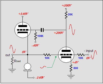 Above, we see the right-top sub-portion of the push-pull OTL amplifier. The constant-current source replaces the bottom output tube and the rightmost triode controls the top output tube’s output, as the input signal is inverted at this amplifier’s output. Thus, any distortion at the output will be presented to the rightmost triode’s grid, which in turn will be greatly amplified and inverted at its plate, where it will drive the top output tube in the opposite direction. For example, a small positive-going pulse applied to the output will create a large negative-going pulse at the top output tube’s grid, forcing its cathode to swing negatively, countering the positive pulse. Now, we can reassemble the OTL output stage, combining these two single-ended sub-circuits into a push-pull amplifier.
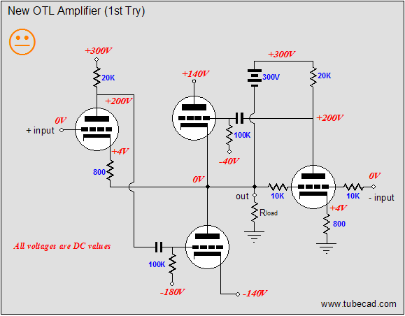
So, what is wrong with this topology? The big problem is that the bottom output tube receives far more drive and correction signal than the top output tube does. Remember that the amplifier’s output swings in-phase with the top output tube’s cathode and grid. This means that the top output tube’s grid must see a much larger input signal than the bottom output tube. Additionally, the two 10k feedback resistors define a 50% voltage divider, which means that 50% of the error signal is lost. So how do we restore balance to this OTL amplifier? What we need to two major changes. THe first is to reference the rightmost triode’s output (its plate resistor) to the OTL amplifier’s output: bootstrapping, in other words. In the schematic above, we see a 300V battery attaching to the output and the rightmost grounded-cathode amplifier’s plate resistor. (Of course, a battery is not likely to be used, but a large-valued capacitor or zener diode would more likely be used.) The bootstrapping will help a great deal in increasing the gain and feedback ratio of this driver tube. And as the circuit stands, it would be enough for most high-end audio companies to start thumping their chests, proclaiming the perfect amplifier, and writing their glossy ads. But does it go far enough to establish balanced operation? No. Well, at least not enough for me. Let's go to work on the left side of the circuit with the second major change.
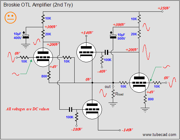
Now, this OTL amplifier just became a bit more interesting. Two additional resistors (10k and 10k) have been added to the left side of the schematic. Their purpose will confuse many, so I will have to slow down a tad now. Let’s revisit a small positive-going pulse applied to the output and let’s imagine both inputs grounded. The pulse now sees two 50% voltage dividers, as each divider is made up of equal-valued resistors. On the right side, the 50% of the pulse’s magnitude is presented to the rightmost triode’s grid. Assuming a gain of ten for this grounded-cathode amplifier, a 1-volt positive pulse will result in a -5V pulse on the plate. On the left side, the 1-volt positive pulse will result in a +0.5V pulse on the leftmost triode’s grid and a 1V pulse on its cathode. Thus, if we once again assume a gain of ten for this amplifier stage, this input tube’s plate will try to swing +10 volts and -5 volts at the same time, so the net swing equals +5V. The top output tube’s conduction is cut by -5V pulse and the bottom output tube’s conduction is increased by the +5V pulse; thus both output tubes work equally to force the output back in line. Perfect balance at last? No. Remember that the top output tube also sees a +1V pulse on its cathode, which must be added to the -5V pulse, yielding a net -6V pulse. Thus, the output-stage is unbalanced, as the bottom output tube only sees the +5V pulse. Or does it? The assumption hidden here is that, with the same plate and cathode resistor values, grounded-cathode amplifiers and grounded-grid amplifiers have the same gain; they don’t. The formula for the gain of a grounded-cathode amplifier is: Well, now that we have pretty much restored balance, we move on to a new problem: poor negative-power-supply-rail noise rejection. The schematic below illustrates the problem.
A triode holds two inputs that allow gain to be realized: the grid and the cathode. In fact, the cathode offers slightly higher gain. (Remember this every time you add a bypass capacitor to a cathode resistor.) This means that if the bottom output tube’s grid sees no power supply noise but the cathode does, the negative power supply rail noise will be amplified by the bottom output triode. Eliminating this leakage of negative PS rail noise into the output requires either noiseless power supply rails or some clever Aikido technique. Guess which answer I suggest. If the bottom triode’s grid sees the same negative-power-supply rail noise as its cathode does, then there is no difference to be amplified. How is this feat accomplished? All that is required is that the leftmost filter capacitor (10µF) have its termination moved to the negative power-supply rail, which will impose the negative power supply rail noise on the top of the leftmost 20k plate resistor, producing much of the noise on the leftmost triode’s plate. Shouldn’t it be all of the rail noise, not just most of it? Yes, indeed, it should; unfortunately, the triode's low rp works against us here. But this simple rearrangement will provide a much less power-supply noise making it to the output, which the feedback can work on to reduce even further. (A pentode-based driver amplifier would work even better at reducing power supply noise, as the pentode’s plate offers a much higher plate resistance than the triode does, which means less voltage division obtains; a cascoded stage would also work well. For the truly advanced practitioner, loading the leftmost triode's cathode with a noise-modulated current source would be ideal.)
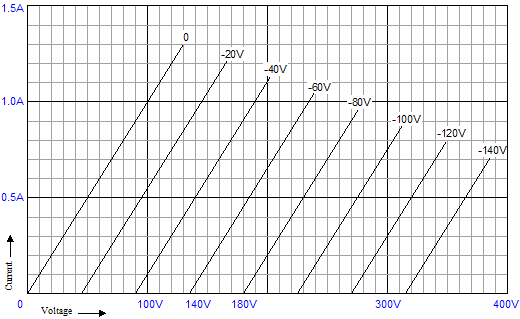
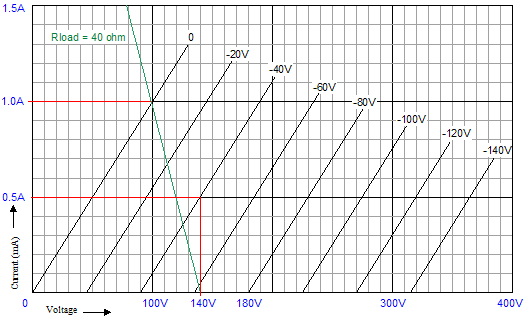
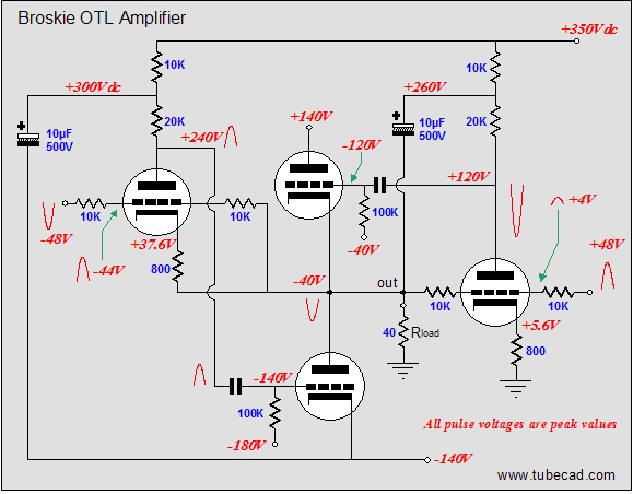
Now, let’s move on to how this OTL amplifier handles a large AC signal. I had a make-believe (perfect) power triode in mind, as I drew the following schematics, whose rp equals 100 ohms; mu, 2.25; and transconductance, 22.5mA/V.
The load resistance equals 40 ohms.
The simple formula, Dividing the maximum current swing by 2 gives us our idle current: 500mA. (Yes, 500mA. We are designing a true, honest-to-God, class-A amplifier.) So, by inspecting the plate-curve graphs above, we see that -40V is needed as a bias voltage and that a negative grid voltage swing of 80V will turn off this triode when 180V sits on its plate. (By the way, 180V/80V = 2.25, the mu in other words, as the amplification factor is the measure of the relative effectiveness of the grid over the plate in controlling current flow through the triode, so whatever amount of current that 180V on plate would induce through the triode can be countered by 180V/-mu, or -80V.)
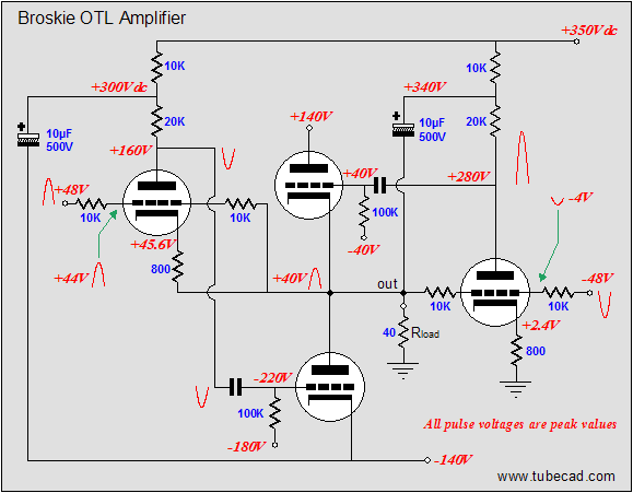
The above schematic shows the voltage relationships needed to achieve a 40V positive swing into the 40-ohm load resistance. Note that the input signal is +/-48V, which means that our two driver-amplifier stages develop a gain of 10 at their plates. Had each driver stage developed a gain of 20, then the input signal need only be +/-44V. Note that the top output tube's grid and cathode share the same voltage (+40V), which means that this tube is fully on and that any further increase in grid voltage will lead to positive grid conduction.
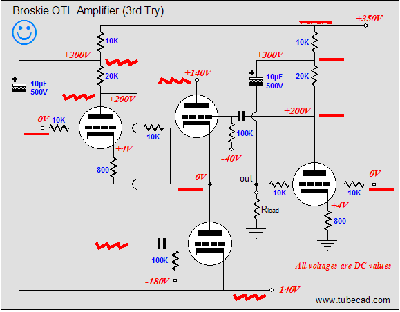
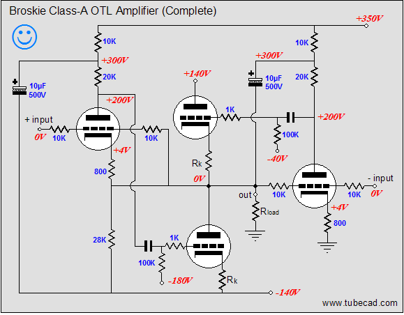
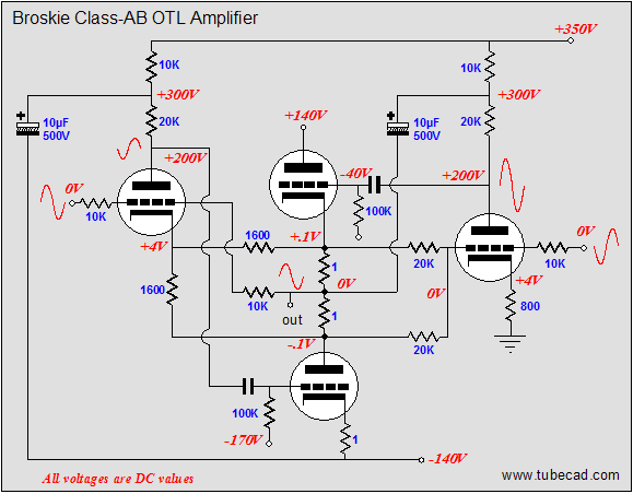
In the same fashion, the schematic above shows the voltage relationships needed to achieve a 40V negative swing into the 40-ohm load. Note how the top output tube sees 180V from its cathode to its plate and how its grid is -80V lower than its cathode. This tube is turned off, while the bottom tube is fully on. (The bottom output triode could conduct even more current, but not without having its grid become more positive than its cathode, which would lead to grid conduction, which is real pain with coupling capacitors and class-AB output-stages. Why would the output-stage's mode of operation figure in the severity of grid conduction problems? Here’s what happens: the coupling capacitor become charged up to a new DC value, as the grid’s conduction effectively defines a low-impedance termination of one end of the coupling capacitor, so as the driver-stage’s plate voltage climbs positively, the coupling capacitor charges up by 5 to 10 volts more than it normally holds. The loud drum smack or whatever lead to the grid conducting passes, but the coupling capacitor now imposes an extra -5 to -10 volts of bias voltage on the output tube’s grid. If the output tubes are biased heavily into class-A, this extra negative bias voltage isn’t a big deal, as in a second or two, the bias voltage will fall back to its set value. In a lean-running class-AB output stage, things do not work out so nicely, as the new negative bias voltage may be enough to turn off the output tubes altogether; never a good idea. The workaround is to DC couple a cathode follower to the output tubes' grids; no coupling capacitor, no problem) Below is the complete Broskie OTL circuit. What's missing is the input-stage and the power supply. The added 28k resistor that parallels the bottom output tube prevents the rightmost triode’s current from flowing through the bottom output tube. The grid-stopper and cathode resistors are safety measures that fools will leave out. The grid-stopper resistors prevent high-frequency oscillations and the cathode resistors prevent current runaway of the output tubes.
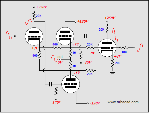
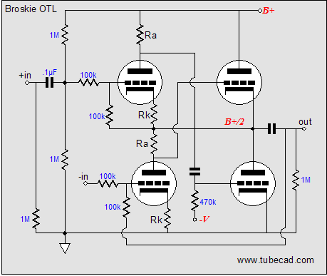
Note the new name, the Broskie Cass-A OTL. As I have posted scores of original circuits in this journal, why is this one labeled with my name? Paradoxically enough, this circuit definitely has the look of one of my circuits; few would not recognize my handiwork in its creation; and yet to my mind (and possibly mine alone), its design seems absolutely fixed by necessity, as any omission or deviation results in worse performance. What about mono-polar power supplies, would this topology work well with a single power supply voltage? With the addition of a coupling capacitor or two, this topology can readily be reconfigured to work with a single B+ voltage. In fact, as the schematic below makes clear, an extremely fine, simple, unity-gain, balanced to unbalanced buffer can be made within the Broskie OTL topology framework.
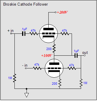
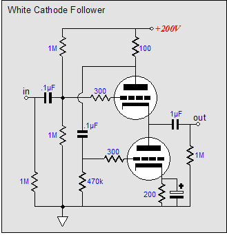
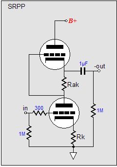
(Imagine a 12AX7 and a 6H30; or a 6SL7 and a 6AS7.) Note the direct coupling of the top output triode’s grid to the bottom tube's plate-resistor, although an additional coupling capacitor might be a more practical approach. This circuit looks like a blend of the Broskie cathode follower, the White cathode follower, and the SRPP. The Broskie cathode follower accepts a balanced input and delivers an unbalanced output; the White cathode follower is a push-pull, non-inverting, unity-gain buffer; and the SRPP is an amplifier that inverts the input at its output and directly couples its top triode to its bottom triode.
Now, all that is left is to revisit the de-notched, Broskie class-AB OTL. Where the class-A version used a single 800-ohm cathode resistor for the leftmost triode, this version uses two 1,600-ohm cathode resistors, which in parallel equal 800 ohms. These resistors not attach to the output, but to the two 1-ohm current-sense resistors that do attach to the output. Correspondingly, the single 10k resistor that bridged the output to the rightmost triode’s grid has been replaced by two 20k resistors, which also attach to the two current-sense resistors, and which equal 10k when placed in parallel.
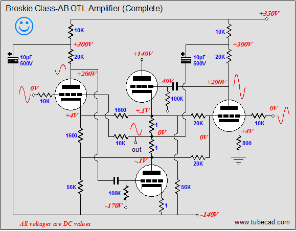
So, are we done? No, one problem still remains: the current that flows through the rightmost triode flows through ground, its cathode resistor, the triode itself and its plate resistor; the current that flows through the leftmost side flows through the bottom output tube, then travels up through the two cathode resistors, the triode, the plate resistor. This is not balanced. It may not make much difference when 500mA flows through the bottom triode and only 5mA flows trough the leftmost driver triode, but it would be significant when only 20mA flows trough the bottom triode (imagine a 6N1P and a 5687).
In the above schematic, we see two new resistors, each with a value of 56k. These resistors combined will draw 5mA from the -140V power-supply rail, which is the amount of current flowing through the leftmost driver triode.
//JRB
|
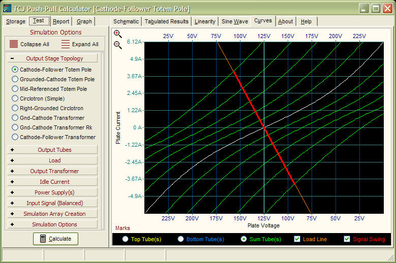
Support the Tube CAD Journal & get an extremely powerful push-pull tube-amplifier simulator for TCJ Push-Pull Calculator
TCJ PPC Version 2 Improvements Rebuilt simulation engine *User definable
Download or CD ROM For more information, please visit our Web site : To purchase, please visit our Yahoo Store:
High-quality, double-sided, extra thick, 2-oz traces, plated-through holes, dual sets of resistor pads and pads for two coupling capacitors. Stereo and mono, octal and 9-pin printed circuit boards available.  Aikido PCBs for as little as $24 http://glass-ware.stores.yahoo.net/
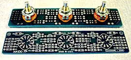
The TCJ Stepped Attenuator The center knob controls both channels, and offers six large decrements; the flanking knobs offer six fine decrements for each channel, creating a volume control and balance control in one easy-to-use stepped attenuator. This clever attenuator uses fewer resistors (only 32) than would be expected from a conventional 32-position stepped attenuator, as two series attenuators would need a total of 72 resistors; and two ladder attenuators would require 140 resistors. In addition, the PCB holds dual sets of resistor pads, one wide and one narrow, so that axial (composition, wire-wound, and film) and radial (thick-film and bulk-foil) resistors can be used without extra lead bending. Although designed to go with the Aikido amplifier, it can be used anywhere a high-quality attenuator is needed, whether passive or active. For example, it would make a first-rate foundation to an excellent passive line box. Visit our Yahoo Store for more details: http://glass-ware.stores.yahoo.net/
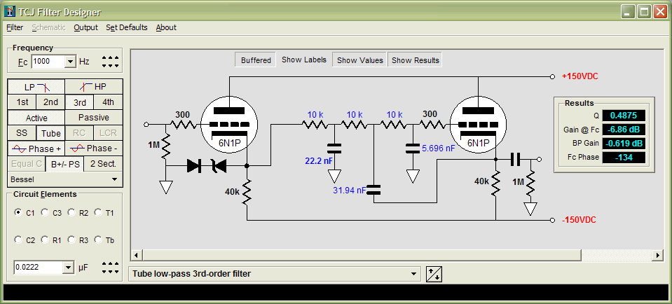
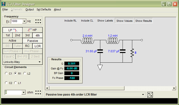
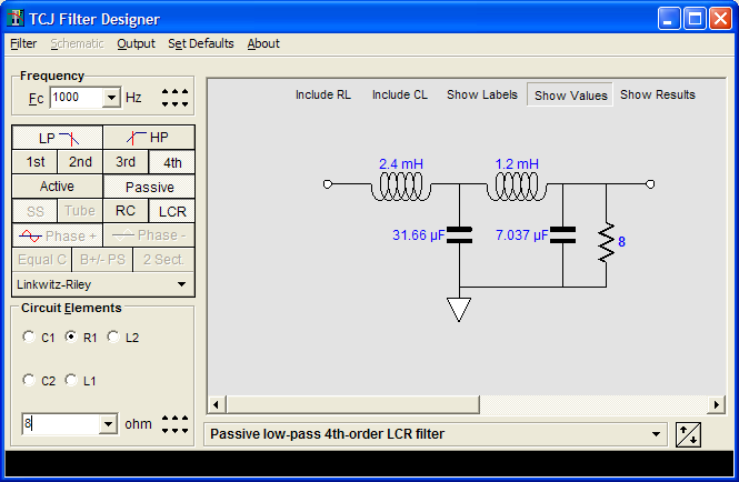
The Tube CAD Journal's first companion program, TCJ Filter Design lets you design a filter or crossover (passive, solid-state or tube) without having to check out thick textbooks from the library and without having to breakout the scientific calculator. This program's goal is to provide a quick and easy display not only of the frequency response, but also of the resistor and capacitor values for a passive and active filters and crossovers. TCJ Filter Design is easy to use, but not lightweight, holding over 60 different filter topologies and up to four filter alignments: While the program’s main concern is active filters, solid-state and tube, it also does passive filters. In fact, it can be used to calculate passive crossovers for use with speakers by entering 8 ohms as the terminating resistance. Click on the image below to see the full screen capture.
Tube crossovers are a major part of this program; both buffered and un-buffered tube based filters along with mono-polar and bipolar power supply topologies are covered. Available on a CD-ROM and a downloadable version (4 Megabytes). Download or CD ROM
|
|||


| www.tubecad.com Copyright © 1999-2006 GlassWare All Rights Reserved |