| John Broskie's Guide to Tube Circuit Analysis & Design |
22 October 2006
Implementing Schematics
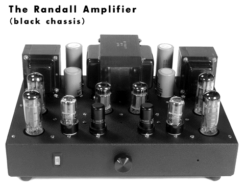
How do I build... Unfortunately, tube gear isn’t cheap, so building it themselves is the only viable solution for many. But at the same time, the glory days of great kits from Heathkit and Dynaco are long past. What we are left with is a much more demanding task, building tube projects that require much more from the builder, as he must construct his own chassis, power supply, PCBs, wiring harness,… In addition, he must know how to solder and wire a project; and should the project not work, he must be able to do his own troubleshooting and repair. While DIY forums help the novice constructor a great deal, they are not perfect (really, there is only so much aid that the Internet can provide to what is a hands-on undertaking). All in all, it is amazing that any tube-based project gets built at all. (The best case scenario is what my friend John Atwood preformed a decade ago, when he sold a single-ended power amplifier kit—the Randall Amplifier—and construction class as a package.
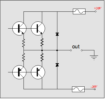
The kit included all the parts that were either hard to make or hard to get, and all the kit builders were gathered in a room for a build-a-thon, with John directing, informing, and overseeing the construction. This is the way to do it, if you have the population density to pull it off—how many good people did God ask for in return for not destroying Sodom and Gomorrah? [Don’t remember? Check out Genesis 18:23-32.] Well that’s the same amount required to pull off a build-a-thon. This means that if you live in Alaska or Wyoming, you are own your own again.) Therefore, depending on your perspective when approaching a tube building project, the schematic is either the most important aspect…or the least. The schematic, however, is just about all that I can provide when answering an email that starts “How do I build ____?” Without the project before me, I cannot list the number and lengths of connecting wires needed or how to quell a ringing output stage. No doubt, my schematic-filled answers fail to provide much satisfaction for far too many. An added wrinkle is that, since my aim is to educate, I often pre-filter the schematics that I post in my blogs. Much like the tour guide who only points out the scenic highlights and ignores the uninteresting 99% of the trip, I often leave out ancillary circuit elements, which would otherwise get in the way of understanding. Hitting the right balance isn’t easy. Too little detail, and the circuit may not work; too much, and few will understand how the circuit works. Here is an example. I always add two rectifiers to the output of my solid-state OpAmp and power amplifiers. See the following schematic:
These rectifiers protect the output stage from inductive kickback damage. Should a high-voltage spike travel back through the speaker cable to the output stage, it will be shorted into the power supply rails. In other words, the output devices will never see a voltage greater than the power supply rail voltages. Considering that these two diodes cost so little (10 to 25 cents each), it would be crazy not to add them to an actual power amplifier. But should they be added to the amplifier’s schematic? If you already know why they are there, they will dissolve into the background; on the other hand, if you do not know their purpose, you might become confused, imagining that the amplifier would not work without them, supposing that they were crucial to setting the idle current or decreasing distortion. I could list an easy 100 other little details that often are left off the schematic, but the more interesting question is, What do I always include? Grid resistors and grid-stopper resistors are always shown. Why? They are the cheapest, easiest way to prevent a lot of headaches and grief when assembling tube gear. Protection diodes that span grid and cathode are often included. These diodes protect the tube by preventing the grid from becoming too positive relative to the cathode, such as at startup, when the tube is cold and DC coupling can present the full B+ voltage to the grid, while its cathode remains glued to ground, such as when a ground-cathode amplifier DC couples into a cathode follower. (These diodes are sometimes called Tube CAD Journal diodes, but their inclusion in tube circuits predates my birth.) Occasionally, a few other schematic details are included when their absence would prove either too dangerous or risky. Another schematic limitation (and a huge fear of mine) is schematic typos. I, for one, am surprised how often I spot schematic typos in electronic books, magazines, and user manuals. I have pointed out a few in past blog entries. Moreover, I must admit that I have posted faulty schematics and I thank all those who have pointed them out to me. What if you cannot spot schematic typos, how do you proceed? A friend once built a tube power amplifier based on a schematic in an old electronic textbook. He performed a masterful job, building a solid, well laid out amplifier; showcase execution. How did it sound? It didn’t, instead the input tube, a 12AX7, would glow bright red. It turns out that the input tube’s grid resistor was terminated into the B+ voltage, not ground. Fortunately, the amplifier was capacitor coupled at the input, so no other piece of equipment was damaged. After I had rewired the amplifier, my friend told me that the resistor had to attach to the B+ and that the schematic said so. He was right; the schematic held one nasty typo. It actually took quite a bit of persuading to get him to go along with the correct wiring; such is the power of the printed page. In the absence of understanding, only pleas based on authority can persuade. On the other hand, if he had understood how the amplifier topology worked, he wouldn’t have needed my help.
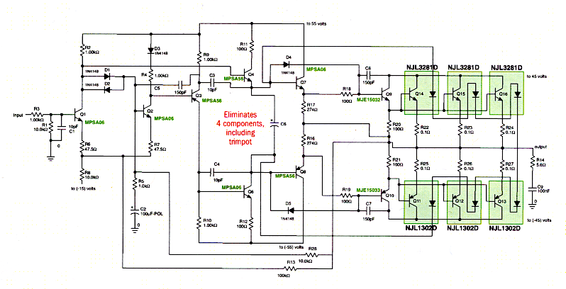
All of which leads in a meandering way to the following schematic:
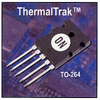
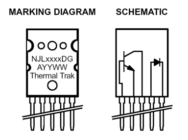
ThermalTrak output devices So, what is so special about housing a power transistor and biasing diode in the same package? Transistors are not like tubes: they do not softly make the transition from off to on, which makes setting the transistor output-stage idle current a critical and troublesome endeavor. (Here is one area where the power MOSFET smokes on the power transistor, as MOSFETs are much less finicky.) What makes the task so difficult is that the target moves. As the amplifier is worked hard or the ambient temperature varies, the transistor’s base-to-emitter voltage varies, nullifying the previous bias setting. Well, with the ThermalTrak™ output transistor these headaches do not arise, as the internal biasing diode tracks its mated transistor, exhibiting the same drift, so the output transistor cannot drift away from its reference. Moreover, the usual bias potentiometer is no longer needed, which increases reliability and decreases cost and effort in the amplifier manufacture. From the ON Semiconductor PDF.
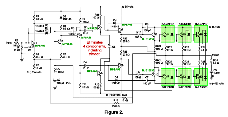
So what should have the schematic looked like? The following schematic appeared in the ON Semiconductor design application PDF for the ThermalTrak™ transistors.
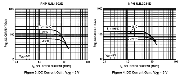
Now, this amplifier will work, from input to output. The two diodes, D1 and D2, are there to protect the input transistors, as they limit the maximum voltage differential between bases to only 0.7 to 0.8 volts. Interestingly, the long-tailed input differential amplifier finds no constant-current source to the negative power supply rail. Why not? The constant-current source is not really needed in this topology, as the driver stage is a push-pull one, so whatever power supply noise that is superimposed upon resistors R2 and R4 will be rejected by the driver stage. (Many solid-state power amplifier use single-ended input and driver stage, leaving only the output stage to push and pull the signal.) The six internal diodes define the output-stage voltage reference for setting the idle current. All in all, not a bad amplifier. Okay, so it is a clever solid-state amplifier design, what does it have to do with tubes? Nothing, unless you want to build a hybrid amplifier. If a hybrid amplifier is your goal, however, these new transistors can solve a lot of problems. The fact that the devices can be bought for less than $2 each only adds to their appeal. (Of course, if you are insulted by their low price, I am sure that one of the high-end parts catalogs will be willing to sell them to you for $50 each). Furthermore, these transistors are linear where it counts: hfe current gain versus collector current. The above graphs show a flat current gain for the first 3A of current in the PNP transistor and up to 4A to 5A for the NPN transistor. Considering that several output transistors will be used in parallel, the 3A window expands to 9A. By the way, 9A into an 8-ohm load equals 324 watts. In other words, a great 100W amplifier could be made with these devices and a +/-45V power supply. Why not a 324W amplifier? Although the NJL3281D (NPN) and NJL1302D (PNP) are 15A, 260V, 200W devices, 200W transistors, unlike 200W tubes, cannot long withstand 200 watts of dissipation. Design conservatively, listen long. So, how do we hook up the tubes? Well, it depends on the class of operation you wish the run the output stage in. For example, if you want to run an efficient, cool-running class-AB output stage, then the following topology would be one possible answer.
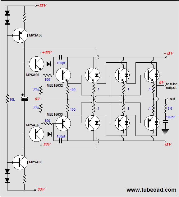
On the other hand, if you want to go for pure, sweet-sounding class-A operation, then an extra pair of output devices is needed (maybe two pairs), so as to increase the reference voltage defined by the diodes in series (each diode holds about a 0.7V voltage drop). Note that the input of this power buffer is found at the center of the diode string. Why? The diodes off a low internal impedance and the center of the diode string is at 0V. Why are the 150pF capacitors included, in this schematic and the original On Semi schematic? No doubt to damp some oscillation problem, but why do they terminate into the power supply rails and not ground? In a feedback-free amplifier, they may not be needed at all. (The two diodes that meet with these capacitors are there to prevent the driver stage from overdriving the output stage.) Which tube front end should be used? If you haven’t guessed that I would say Aikido, you must new to this blog. Of course, about a hundred other possible tube topologies could be used. No matter which tube circuit is used, some form of DC offset correction circuitry will be needed, maybe as little as one potentiometer and a few resistors. Okay, who is going to be the first to try making a hybrid amplifier with these interesting power transistors? You have the schematic, what are you waiting for? //JRB
|
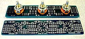
The TCJ Stepped Attenuator The center knob controls both channels, and offers six large decrements; the flanking knobs offer six fine decrements for each channel, creating a volume control and balance control in one easy-to-use stepped attenuator. This clever attenuator uses fewer resistors (only 32) than would be expected from a conventional 32-position stepped attenuator, as two series attenuators would need a total of 72 resistors; and two ladder attenuators would require 140 resistors. In addition, the PCB holds dual sets of resistor pads, one wide and one narrow, so that axial (composition, wire-wound, and film) and radial (thick-film and bulk-foil) resistors can be used without extra lead bending. Although designed to go with the Aikido amplifier, it can be used anywhere a high-quality attenuator is needed, whether passive or active. For example, it would make a first-rate foundation to an excellent passive line box. Designed by John Broskie & Made in USA Visit our Yahoo Store for more details: http://glass-ware.stores.yahoo.net/
|
|||


| www.tubecad.com Copyright © 1999-2006 GlassWare All Rights Reserved |