| John Broskie's Guide to Tube Circuit Analysis & Design |
|
14 December 2017 Post 405
Constant-gm Math Let's start with the conventional two-transistor emitter-follower output stage.
The two voltage references (the two batteries in the schematic) provide the needed bias voltage to turn on the two transistors. How much turning on depends on how high an idle current we wish to impose. At one extreme, we go the full Monty and run a heavy class-A idle current, where the idle current must equal half of the peak expected output current swing. At the other extreme, we use thinnest trickle of current we can get away with, as it will result in the least amount of heat at idle. In other words, we get as close as we can to class-C without out actually turning off the transistors—in other words, class-B, which is a wierd limbo state between being on and being off. The late Randy Slone-whose book, High Power Audio Amplifier Construction Manual, should be read by everyone interested in solid-state amplifier design along with Bob Cordell's book, Designing Audio Power Amplifiers-referred to this lean output stage operation as a "push-cutoff" stage, as he preferred to reserve the "push-pull" label for only that portion of output stage operation where both output device were still conducting, which in a class-A stage meant 100% of the waveform. As you might expect, the ultra-lean push-cutoff class-B output stage suffers from higher distortion than a heavy-current push-pull class-A output stage. If the idle current falls too low, the output transistors cutoff and gross crossover distortion occurs, as a portion of the output signal isn't produced; if the idle current is set too high (rich class-AB), gm doubling results, which also produces distortion, not anywhere as much as class-C operation; so if an output stage is going to err, let it be in the class-AB side. So, if class-A is heaven, class-C is hell, and class-B is limbo, what is class-AB? Purgatory, perhaps.
Nonetheless, this simple output stage configuration offers a lot of advantages, which is why 99.9% of solid-state power amplifier employ this topology or some variation on it, such as the paralled emitter-followers shown above or the Darlington configuration, as shown below.
A popular variation is the following.
Another popular variation is the famous triple, as shown below.
By greatly unloading the voltage-amplification stage (VAS or driver stage), much lower distortion results, as far greater open-loop gain is created, which in turn allows for more negative feedback to clean up the output signal. Indeed, Andy Slone argued that the distortion produced by the simple emitter-follower pair was particularly well-suited the negative feedback clean ups. Why? Because the simple emitter-follower pair is so dang stable. No gain, just unity-gain buffering. It offers 100% degenerative negative feedback right where you need it: where the loudspeaker attaches to the amplifier.
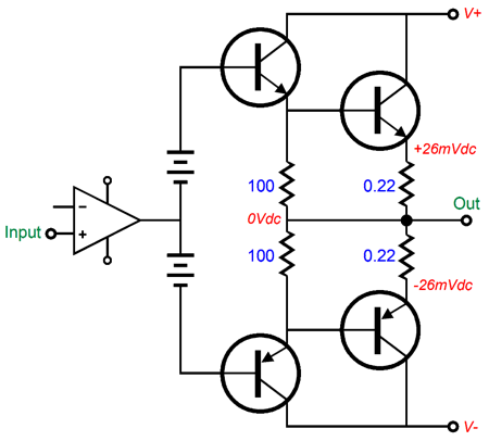
If you ever have lived with or worked with or traveled with an unstable individual, then you know just how desirable stability is. In analog electronics, stability usually means no high-frequency oscillations, which means no undesired phase shifts. Oscillations are a pain to deal with and to banish. The worst are the random it's happening, no it's not, wait a second it is... Interment problems are always a pain; for example, the car noise that stops when you bring your car to the mechanic and reappears as you drive home. On your test bench, no oscillations, but in your living room, wild oscillations taunt you; back on the bench, the oscillations cannot be seen. Why? If only you knew. Perhaps, the living room light dimmers interject sharp pulses into the wall voltage that set off the oscillations. Or perhaps, your speaker cables or loudspeakers or interconnects or line-stage amplifier or... the list goes on and on. With oscillations in mind, let's return to the complementary-feedback variation, where four transistors are used, two masters and two slaves.
Transistors Q1 and Q2 are the masters, with transistors Q3 and Q4 enslaved. Effectively, we have created a super emitter-follower, as the two input transistors Q1 & Q2 encompass the two output transistors, Q3 & Q4, which are configured as common-emitter amplifiers. The result is vastly lower output impedance and increased linearity. In addition, this arrangement takes care of the problem of beta droop, where the output transistors lose current gain at higher current flows. Sounds wonderful doesn't it. And it is, which is why this configuration is often used in electronics, but power amplifier output stages throw a bunch of problems our way. The transistors hold base-to-collector capacitance, so better schematic would look like the following.
Note that these two capacitances impose cascading phase shifts. Almost all solid-state power amplifiers that are not class-D types run in class-B or class-AB. This makes for much smaller, lighter power amplifiers, as massive power transformers and hulking heatsinks are not required. This also means, however, that the output transistors must be turned on and off; in contrast, in a class-A power amplifier, they never turn off. Well, in the complementary-feedback output stage, the power transistors are easy to turn on, as transistors Q1 & Q2 need only draw some extra current; turning these output transistors off, on the other hand, is not easy, as so little current flows through the 100-ohmm collector resistors. Some place an emitter follower stage in between the compound pair.
If power MOSFETs are used as the output devices, then the emiter's load resistor can be replaced by a constant-current source, as the MOSFET turn-on voltage is great enough to contain a constant-current source.
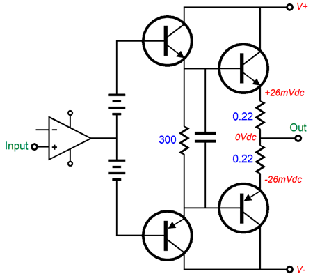
Some double up on the compounding gain stages within the feedback loop.
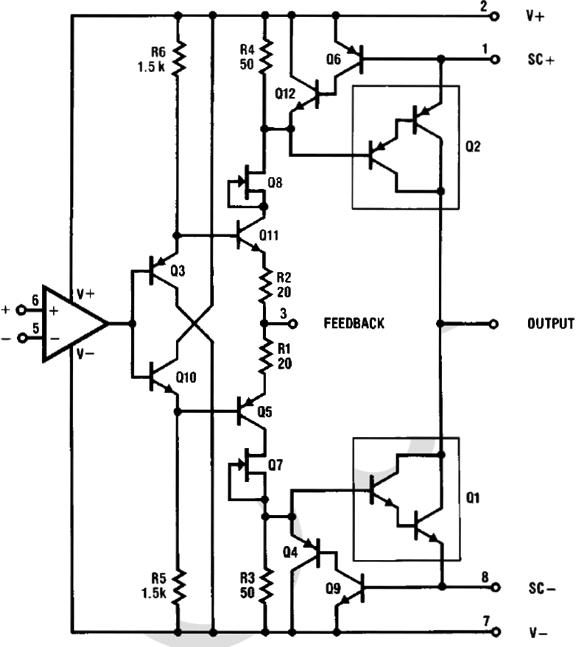
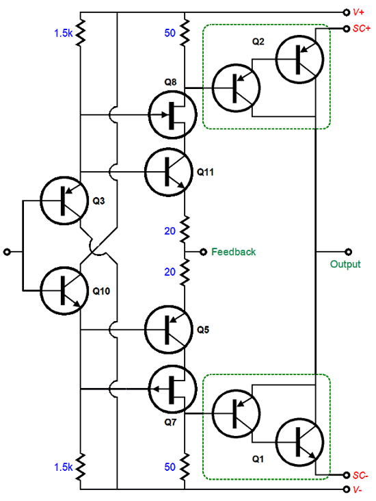
We have moved quite far from the simple emitter-follower output stage, but if you stare at the above schematic, you will see that transistors Q1 and Q2 are effectively super transistors that are augmented by transistors Q4 through Q6. So, in a way, we haven't traveled that far from the emitter-follower output stage. There is one key difference, other than stability issues. The simple two-transistor, emitter-follower output stage, however, allows a for a clever trick to minimize gm doubling by carefully selecting emitter resistor values and idle current, which was proposed by Dr. Bernard Oliver who was the vice president of research at Hewlett Packard and who spelled out the way to avoid crossover distortion in his 1971 paper, Distortion in Complementary-Par Class-B Amplifiers. This technique, however, is not applicable to the complementary-feedback pair; if anything, the two local negative feedback loops make for even sharper turn-on/turn-off glitches, so less averaging can obtain. At the same time, I must point out that making this trick work in practice with the simple emitter-follower output stage is difficult, as the output transistors in the emitter-follower pair do not exhibit a constant base-to-emitter voltage, but a varying voltage that depends on how hot the transistor is. If you have ever tried to set the bias voltage on a transistor class-B amplifier, you soon discover that the target moves. Sounds like a simple problem to fix, but it isn't. The voltage-multiplier circuit used to set the base-to-base voltage in the output stage must thermally track the output device temperature, which isn't easy. The heatsink is slow to heat and slow to cool, so this thermal lag throws off the voltage-multiplier circuit, making respond too late and then over compensate when the devices have cooled. You set the idle current at idle, then play some Led Zeppelin, then measure again and the idle current is off. And if you try setting the bias voltage with the aid of a distortion analyzer, you discover that the lowest-distortion setting differs with output wattage. And if you try setting the bias voltage by ear, you discover that the best sound depends on what is being played and how loudly. Moreover, Oliver's math requires that if the target emitter voltage is 26mV, then 21mV or 31mV won't do. So, is the complementary-feedback pair complete junk? No, not at all. It does offer some real advantages in a class-A power amplifier. And, paradoxically enough, it offers the potential of a super-lean class-B output stage. Where a emitter-follower output stage might require 150mA of idle current, a complementary-feedback pair could use as little as 10mA, as Douglas Self pointed in his 1999 article, titled Cool Audio Power, in Electronics World magazine, August 1999, p657. (In general, the complementary-feedback seems to be much more popular in Great Britain than here in The States. Why? Perhaps the smaller listening rooms require fewer watts and the complementary-feedback pair often offers lower distortion at 1Vpk output than the simple emitter pair.) Moreover, the complementary-feedback pair allows for voltage gain, which the emitter-follower cannot provide. This proves particularily important when using MOSFETs as output devices, due to their relatively high turn-on voltages. In addition, we can use a nested negative feedback loop on just the output stage. Here is an example from the National Semiconductor LH0101, which sadly is no longer made; it can be bought NOS, however, for about $450 each. (A dang shame, as the amplifier held a FET input stage and was unity-gain stable and could put out peaks of 5A, with 2A steady output.)
Note that we could either employ 100% feedback by attaching pin 3 to the output (100% feedback just for the output stage, not the entire amplifer) or we could use a two-resistor negative feedback loop to apply less negative feedback to the output stage. The only parts that confuse me are the two FETs, Q7 & Q8. I do not see how they can add anything useful. In fact, they appear detrimental to me. Perhaps this is what they meant to show:
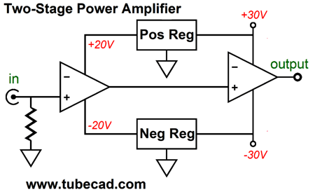
Now the two FETs create cascoded stages. Of course, we are free to roll our own version of the LH0101. This would allow us to replace the Darlington output transistors with MOSFETs and break the global negative feedback loop, so the input amplifier got its own feedback loop as would the output stage, which must run with some voltage gain due to the MOSFETs' large turn-on voltages. Why would we want to do all of the above? Long ago, I built a solid-state power amplifier that held two cascading stages, each with its own negative feedback loop, but no global loop around the entire power amplifier.
(Because of fond memories of this experiment, I later tried my naked tube output stage designs, wherein the power amplifier held only output tubes, power and output transformers, but not input or driver tubes. The tube line-stage amplifier provided sufficient voltage gain to drive the single-ended output stage. At one listening session, a friend who was the most conservative tube amplifier builder possible, who never varied from 50 year-old schematics, was wowed enough to make him briefly question is his steadfast devotion to stodgy design practice.) A long introduction, but now we can look at my proposed constant-gm output stage that looks a lot like a complementary-feedback pair, but really isn't one. Four power transistors are needed, not the pair of two medium-power transistors and two power transistors used in the complementary-feedback pair.
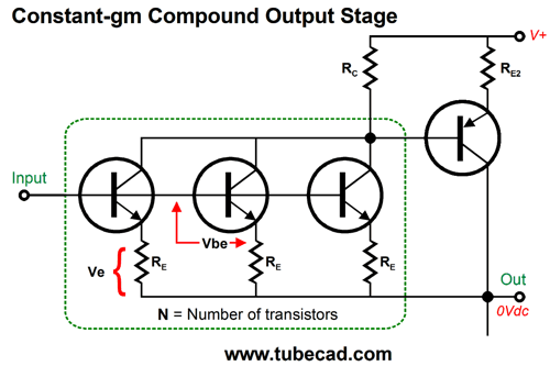
Note how transistors Q1 and Q2 control the turning on and off of transistors Q3 and Q4, but do not complete a negative feedback loop with them, as Q3 and Q4 collectors do not terminate into Q1 and Q2 emitters. If the output signal is small enough, transistors Q3 and Q4 may never turn on. Think of them as a reserve army that is only brought into battle when needed; and when brought in, double the force forthcoming. In other words, this arrangement results in a two-slope output device.
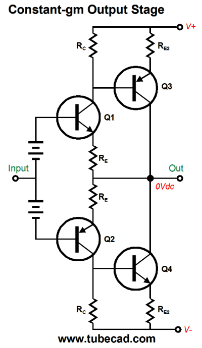
At idle, only transistors Q1 and Q2 are conducting, but as they are configured in push-pull, their transconductances combine. As the output voltage swings positively, Q2 will cutoff and Q3 will turn on and its transconductance will add it Q1's to make a constant-gm, a constant doubled gm. As you might imagine, timing and resistor ratios must be carefully adjusted for optimum operation. By the way, it is worth noting that the problem the complementary-feedback pair faces of turning off its output transistors does not apply here, as the collector resistor values are hundreds of times smaller in value in the constant-gm configuration. Nor need we worry excessively about stability issues, as no internal negative feedback loops are present. Now, on to the math. The following schematic shows just the top half of the constant-gm compound output stage.
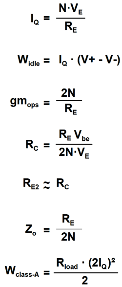
The key variables are labeled. N is the number of primary pairs of output transistors that are used; N could just 1 (one pair) or 3 or 4 pairs. Because we are purposely running a heavy class-AB idle current, with a fat center of class-A operation, we need only add one (perhaps two) gm-doubling transistors (the PNP transistor in the above schematic), as this transistor is off at idle and only conducts when the output requires it.
The power dissipated at idle is found from multiplying the idle current (Iq) against the total power-supply voltage, which is the sum of the absolute values of the positive and negative power-supply-rail voltages. The last formula gives us the amount of class-A power output. In most class-B, transistor-based amplifiers this value is tiny, as in 0.23W tiny. But in the constant-gm output stage, we run such hot idle currents that the class-A power output can be significant, as in 13W big. I would love to see all class-B and class-AB power amplifiers specified by tow numbers: the first being the amount of class-A ouput; the second, the full-output amount. For example, a constant-gm amplifier might sport the specification of 13W/40W. Wait a minute, John, you said that Oliver's math required that if the target emitter voltage is 26mV, then 21mV or 31mV won't do; but aren't you also requiring super fine accuracy? No. For example, say we set the emitter voltage to 300mV; being off by 5mV is only off by less then 2%, whereas in the Oliver setup, it would be almost 20% off. Far more importantly, we have moved the two output transistor cutoffs far away from the 0V center, so the ear is far less likely to complain with the big fat juicy class-A center. The analogy I used ten years ago was: "Consider which would trouble you more: one sore on the roof of your mouth, at the top near your front teeth, within your tongue’s easy reach; or two, far in the back behind your molars?"
Special Thanks to the Special 59 (Lost 2)
If you have been reading my posts, you know that my lifetime goal is reaching post number one thousand. I have 595 more to go. My second goal is to gather 1,000 patrons. I have 941 patrons to go. If you enjoyed reading this post from me for the last 18 years, then you might consider becoming one of my patrons at Patreon.com. It would make a big difference to me. Thanks.
Tubes and Constant-gm
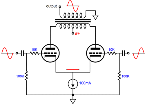
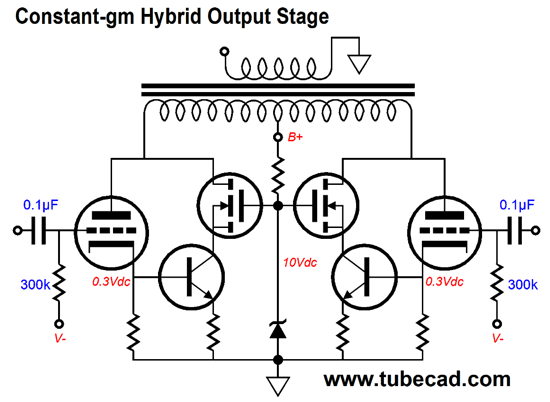
It must run in class-A due to the constant-current source. It runs in 100% class-A mode and both output tubes are always turned on; it also runs in 100% constant-gm mode. The sound is fabulous, but weak due to the limited amount of class-A watts available. The following design runs the output tubes in heavy class-AB and the the transistors in class-C, which means that the transistors are turned off at idle and for the first 10W of output. Once one output tube turns off completely, the opposing side's transistor turns on and provides the needed transconductance boost needed to restore a constant-gm operation.
The NPN transistors can be low-voltage, medium-power devices, such as the MJE200. The MOSFETs, in contrast, must be high-voltage, power N-channel MOSFETs, such as the IXTH1N250. Now, let's flesh-out the design further:
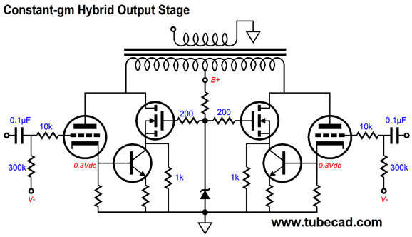
Grid and gate stopper resistors were added, as were two 1k source resistors. Why? We don't want the two MOSFEts to ever turn off, so we give them the 1k resistors to allow some current flow, even when the NPN transistors are turned off. Effectively, at idle the two MOSFETs function as constant-current sources that put out about 6mA of current each. As far as the output transformer is concerned, these two constant-current sources cancel and make no difference to its functioning. We select cathode resistor values that will, at idle, drop half of the NPN transistor base-to-emitter voltage. We then select the emitter resistors that will restore the missing transconductance lost by one output tube turning off. In theory, the emitter resistors would equal the cathode resistors in value; in practice, we would make the emitter resistors slightly lower in value. For example, if the cathode resistors were 3.3-ohm, then we would use 3-ohm emitter resistors. We can apply the same technique to an OTL power amplifier's output stage.
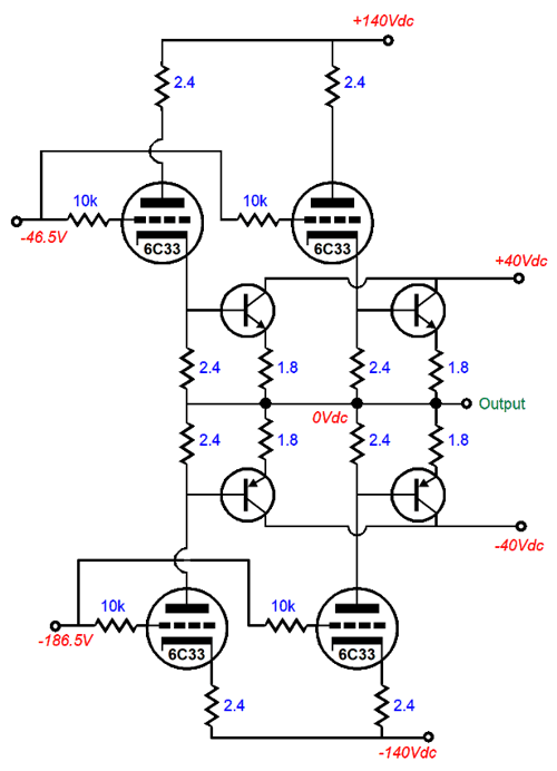
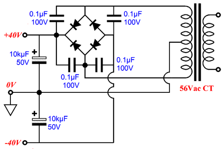
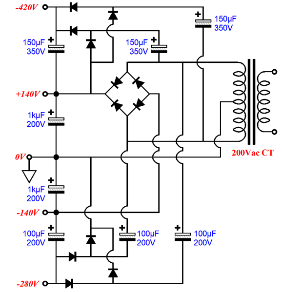
The four power transistors are completely turned off at idle and only turn on when either the top or bottom triodes cut off. The result is both a constant-gm operation and much greater power output, as the number of output tubes has effectively been doubled. Note that the transistors run off of +/-40V power-supply rails, not the +/-140V rails that the tubes run on. Why? The peak output voltage will be only about 32V, so there is no need for any greater power-supply rail voltage for the transistors. A 56Vac center-tapped secondary can be used to create the +/-40Vdc power-supply rails.
This was easy; the rest of the OTL amplifier will require many more rails, as the input and driver stage will require a much higher B+ voltage, while the bottom output triodes will need a negative bias voltage much lower than -140Vdc.
Four rails voltages from one center-tapped secondary, not bad. What is missing are the fuses and some RFI-shunting capacitors across the rectifiers. I better stop now, or this OTL will design will grow to monstrous proportions.
//JRB
User Guides for GlassWare Software
For those of you who still have old computers running Windows XP (32-bit) or any other Windows 32-bit OS, I have setup the download availability of my old old standards: Tube CAD, SE Amp CAD, and Audio Gadgets. The downloads are at the GlassWare-Yahoo store and the price is only $9.95 for each program. http://glass-ware.stores.yahoo.net/adsoffromgla.html So many have asked that I had to do it. WARNING: THESE THREE PROGRAMS WILL NOT RUN UNDER VISTA 64-Bit or WINDOWS 7 & 8 or any other 64-bit OS. I do plan on remaking all of these programs into 64-bit versions, but it will be a huge ordeal, as programming requires vast chunks of noise-free time, something very rare with children running about. Ideally, I would love to come out with versions that run on iPads and Android-OS tablets.
//JRB
|
|
Kit User Guide PDFs
Only $12.95 TCJ My-Stock DB
Version 2 Improvements *User definable Download for www.glass-ware.com |
||


| www.tubecad.com Copyright © 1999-2017 GlassWare All Rights Reserved |