| John Broskie's Guide to Tube Circuit Analysis & Design |
Post 235 26 June 2012 Current to Voltage (part two)
Solid-state devices, on the other hand, offer extremely low input impedances at their emitters (transistors) or sources (FETs and MOSFETs). In addition, even their high-impedance inputs at their base (transistors) or gates (FETs and MOSFETs) can be made effectively low in impedance with negative feedback. Open-loop gain fuels negative feedback and solid-state devices can produce huge amounts of gain, due to their vastly greater transconductance. But let's start with an I-to-V circuit that uses a transistor's emitter as its input.
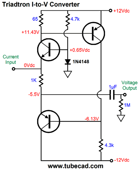
Triadtron I-to-V Converter
Now if a varying current is drawn from the circuit's input, the circuit will strive to maintain a constant current flow through the NPN transistor, so the 1k I-to-V resistor will see a varying current flow, which will create the needed AC signal voltage. If this still seems not to make sense, imagine a 12k resistor bridging the input and the positive 12Vdc power-supply rail. This resistor will draw 1mA, thus the bottom PNP transistor and the 1k I-to-V resistor must draw 6.5mA to keep the steady 5.5mA flowing through the NPN transistor. Now, imagine the 12k resistor spanning from the input down to the -12Vdc rail. The resistor still draws 1mA, but in the other direction, so the bottom PNP transistor and the 1k I-to-V resistor must draw 4.5mA to maintain the fixed 5.5mA through the NPN transistor. Okay, now we can move to a fleshed-out version of this circuit.
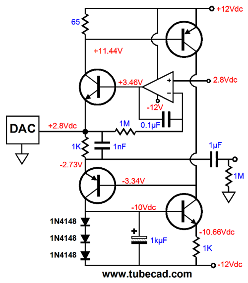
Be honest, if I had started with this schematic, would it have seemed impossible to decipher? The input is at +2.8Vdc this time, not ground level, but lowering it back to 0V is easy enough: just ground the OpAmp's positive input. The 4.3k resistor has been replaced by a constant-current source. The 1k I-to-V resistor has been bypassed by a 1nF capacitor, which will impose a 1st order low-pass filter at 159kHz. I know many are thinking: Sure, John, that's a spiffy little solid-state circuit, but where the heck are the tubes? As is very typical for me, I saved the good stuff for the end.
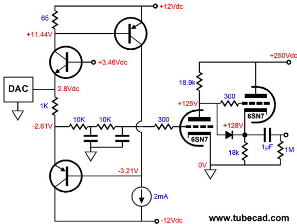
The output coupling capacitor is gone and 6SN7-based tube gain stage follows the I-to-V converter and 2nd-order, low-pass filter. (A much fancier filter can be implemented, as the tube stage allows a MFB filter configuration.) I sure like the look of this circuit. Unlike tubes, low-noise transistors are both cheap and readily attainable. Setting of a differential version only requires twice the parts.
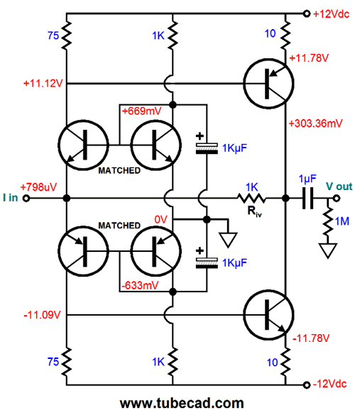
Push-Pull I-to-V
The input NPN and PNP transistors draw about 11mA and any current flow out of (or into) their emitters will be relayed to the two 75-ohm collector resistors, but in anti-phase. In other words, if the bottom resistor sees 1mA more current flow, then the top resistor must see 1mA less current flow. This creates a push-pull operation of the two output transistors, as the output voltage swings up and down to counter the input current through the 1k Riv resistor. Due to the high open-loop gain, almost of the input current audio signal from the DAC will flow through the 1k resistor.
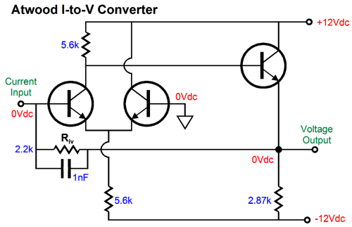
John Atwood's I-to-V Circuit
John purposely designed the most minimalist circuit possible. His circuit can be seen as holding only two transistors, as the transistor with the grounded base is used primarily to refence the input transistor, so its base can be at ground level. Unfortunately, the engineers in Japan were not into using of the fewest devices and barest essentials in their designs, preferring something much more baroque, so John's circuit received an unwanted do-over. John's circuit is, at its core, an inverting OpAmp that uses the Riv resistor to to complete the negative feedback loop. Adding one extra resistor makes this clear, as we now have an inverting voltage amplifier. (Note how the input 1k resistor is effectively a voltage-to-current converter.)
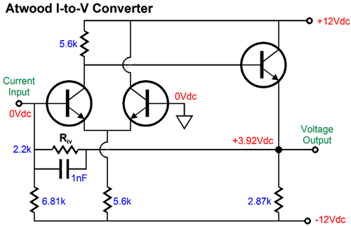
One problem both of these circuits face is that the the output cannot swing down as far as it can swing up. Remember, the input transistor's base isn't supposed to see any voltage swing, being effectively a "virtual ground." John's workaround was to add an additional resistor, which provokes a 4V DC offset at the output.
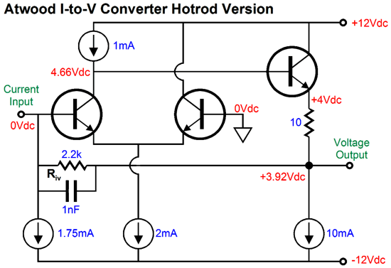
Indeed, the circuit can be hotrodded in many different ways: current mirrors, constant-current sources, emitter resistors—all can be added. The following is a one possible modification.
Assuming that the DAC only puts out a 1mA current swing, this hotrod version should be able to swing the +/-2.2Vpk output voltages. The constant-current sources greatly increase the amplifier's gain and add to the PSRR of the circuit. In SPICE simulations the disortion retained the same harmonic stucture, but fell by -40dB over the stock non-CCS version. A different approach would be to reconfigure the amplifier's topology, which would allow us to forgo the input pull-down resistor.
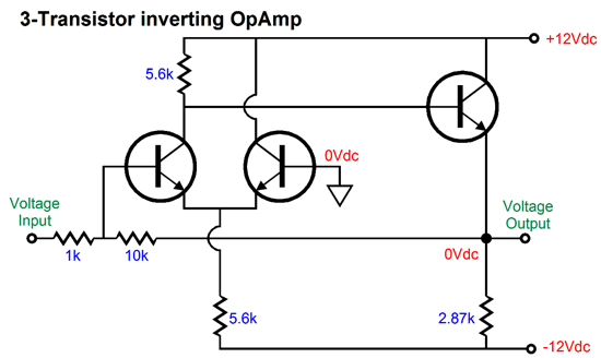
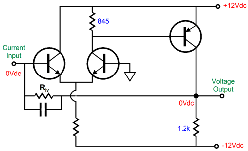
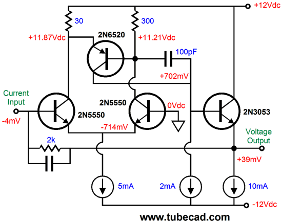
This inverting OpAmp still uses only three transistors, but it holds two gain stages. The result is both higher open-loop gain and much bigger output swings. The higher gain will reduce the input impedance even further. (When actually building such a circuit, it is often a good idea to place a small-valued capacitor from the PNP transistor's base to the the output.) Now, lets look a truly hotrod version, which makes use of Rudolf Lender's topology, made famous by Erno Borbely. (The PNP transistor at the top.)
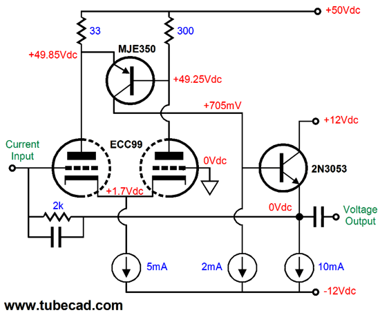
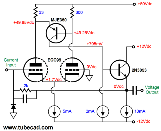
This circuit more effectively uses the differential input stage by having both transistors drive the PNP transistor. The 2N3053 output transistor is run in single-ended fashion and can easily make the swings needed. Okay, once again a nice solid-state circuit, but where are the tubes? Here they are. The transistor differential input stage has been replaced by an ECC99 tube.
The 2N3053 can even be replaced by another ECC99 triode (its plate will attach tot he +50V rail). One problem with this circuit is that the tubes take time to heat up before they will conduct, which means that the output will slam into the negative power-supply rail at startup. The out capacitor protects the line stage or power amplifier that follows, but the DAC will be exposed to the negative input voltage. The workaround is to add a safety diode, which will only conduct when the input falls below about -0.7V.
Once the tubes are hot and conducting, the diode falls out of the circuit, as it is no longer forward biased.
Next Time
//JRB |
I know that some readers wish to avoid Patreon, so here is a PayPal button instead. Thanks.
John Broskie
And
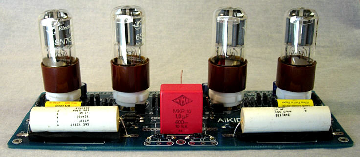
High-quality, double-sided, extra thick, 2-oz traces, plated-through holes, dual sets of resistor pads and pads for two coupling capacitors. Stereo and mono, octal and 9-pin printed circuit boards available.
Designed by John Broskie & Made in USA Aikido PCBs for as little as $24 http://glass-ware.stores.yahoo.net/
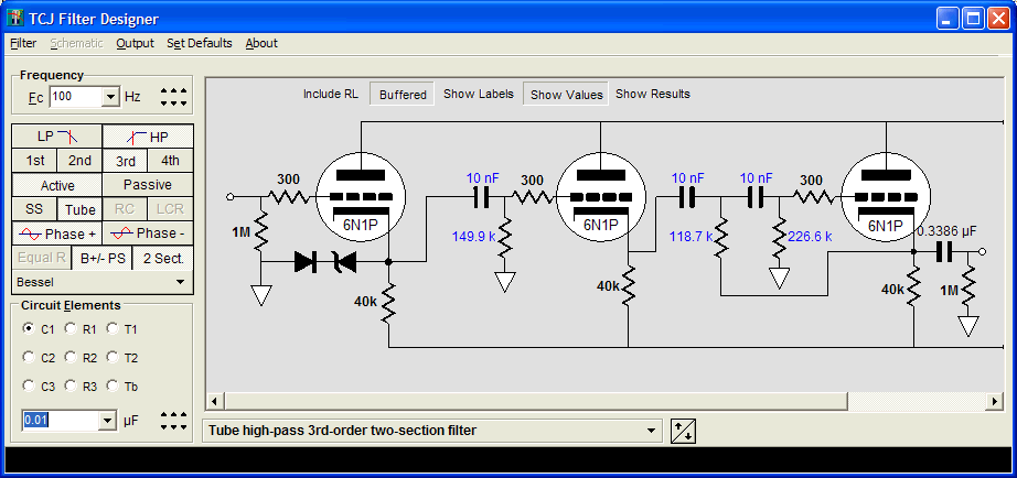
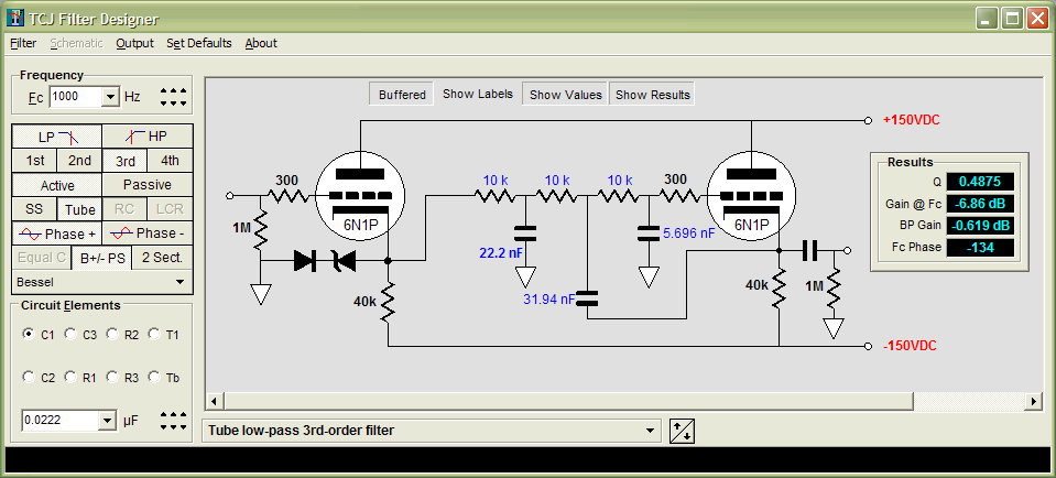
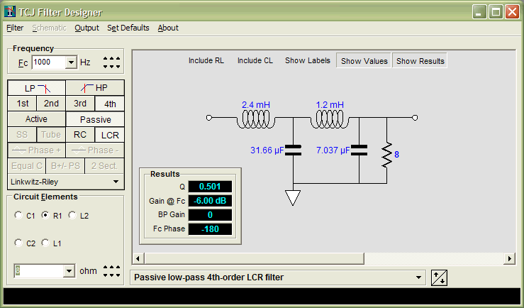
The Tube CAD Journal's first companion program, TCJ Filter Design lets you design a filter or crossover (passive, OpAmp or tube) without having to check out thick textbooks from the library and without having to breakout the scientific calculator. This program's goal is to provide a quick and easy display not only of the frequency response, but also of the resistor and capacitor values for a passive and active filters and crossovers. TCJ Filter Design is easy to use, but not lightweight, holding over 60 different filter topologies and up to four filter alignments: While the program’s main concern is active filters, solid-state and tube, it also does passive filters. In fact, it can be used to calculate passive crossovers for use with speakers by entering 8 ohms as the terminating resistance. Click on the image below to see the full screen capture.
Tube crossovers are a major part of this program; both buffered and un-buffered tube based filters along with mono-polar and bipolar power supply topologies are covered. Available on a CD-ROM and a downloadable version (4 Megabytes). |
|||


| www.tubecad.com Copyright © 1999-2012 GlassWare All Rights Reserved |