| John Broskie's Guide to Tube Circuit Analysis & Design |
|
16 April 2007
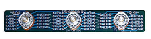
Passive line stages and the TCJ stepped attenuator
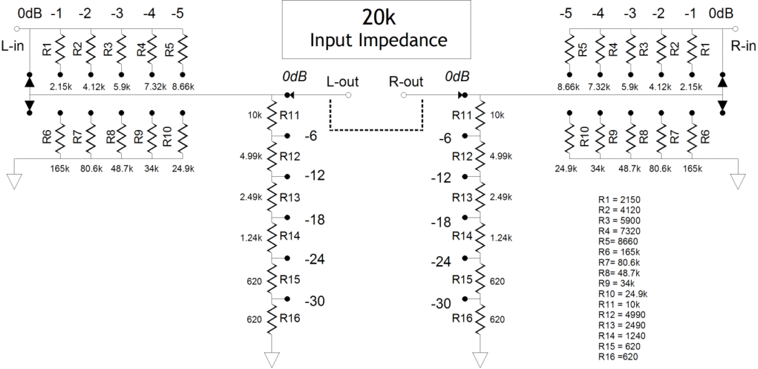
Ideally, less maximum attenuation, finer steps, and a much lower output impedance are needed. Well, that is exactly what I can now offer. The same printed circuit board, three rotary switches, and 32 resistors, except that the new resistor values yield a 20k stepped attenuator with 36 -1dB steps for a maximum attenuation of -35dB and a worst-case output impedance of only 5k, five times less than the 100k version and fives the bandwidth into the same capacitance load.
The price tag is the same embarrassingly-low $29 as the standard 100k attenuator. I cannot honestly think of another $29 investment that will yield as big a sonic bang for the buck. http://glass-ware.stores.yahoo.net/newhardware.html
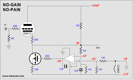
NO GAIN, NO PAIN
The complaint constant-current source is not constant in terms of DC operation, but rather operates at whatever the triode’s idle current happens to be (1mA to 50mA); in AC terms, it's idle current and output impedance look like constant-current source to the vacuum tube it loads. This complaint constant-current source also sets the DC offset to zero volts. In other words, with the cathode follower working into this load, there is no gain, very little distortion, a low output impedance, and no coupling capacitors. Not a bad design. Since the almost ten years that the circuit has been available on the website, several solder slingers have built the buffer. All the response that I have received has been glowing with praise. The one complaint, however, mentioned more than once, troubled me. The DC offset would not stick to zero volts, but would sit 40-120mV above or below 0V. Odd, I remember measuring about 10mV, which is much less than most oil-filled coupling capacitors leak at the output. What went wrong with the readers' buffers? Or, a better question, What went right with my test setup? Back in the late 90s, I lived 30 miles from Silicon Valley. So it was an easy jaunt to the many electronic surplus store that the valley one held, but no longer does. At these stores, it was easy to find and buy them for a ten cents each. What did those super-tight-tolerance resistors buy me? Very little DC offset.
Even 1% resistors are not good enough, as the pair of two-resistor voltage dividers used in the circuit can produce a sizeable DC offset from the 1% resistance error, as shown above. For example, with an LF411/LF412 OpAmp and one voltage divider resistor at 990k and the other at 1.01M, the DC offset will equal 260mV (assuming the worst case for all four resistors). On the other hand, 0.1% resistors yield only a DC offset of 25mV, worst-case. The only problem with 0.1% and 0.01% resistors is that they both expensive and hard to find. One workaround is to buy a handful of 1% resistors and hand select two 0.1% matched pairs (remember the absolute value is not important, only the relative matching). With just 10 resistors, I would expect to easily come up with two tightly matched pairs. The only problem with this workaround, asides from the five minutes of work it entails, is that the 1% resistor just might drift 1% over time, which would throw off our matching efforts. Another workaround is to give the OpAmp a positive power-supply rail, which would obviate the need for the two voltage divider resistors, as shown below. .png) In fact, with the positive power-supply rail, 20% resistors could be used, as no voltage division occurs, only low-pass filtering. (Now that I look at the above schematic, I realize that I should have included the LF412’s own intrinsic DC offset.) Of course, adding an extra power supply rail is a pain, albeit a small one. This lead me to thinking about keeping the single negative power supply rail and not using voltage dividers, as show below. .png)
Will this work? Can both OpAmp inputs be at the positive power supply voltage? The answer can be gleaned from inspecting the LF412’s datasheet (use National Semi’s, not TI’s). The following schematic is from the datasheet and it shows a P-channel FET differential input stage, loaded at the common sources by a constant-current source, with the drains loaded by a current mirror. So far great, as this topology yells out to be careful not to swing the inputs too negatively and that maybe the inputs can be safely referenced to a voltage equal (or greater) than the Vcc voltage (the positive power supply voltage). Had a pair of N-channel FETs been used in place of the P-channel FETs, the opposite would be true. 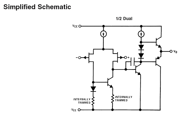 And, of course, had a pair of PNP transistors been used in place of the FETs, the inputs would have to be bound well within the Vcc voltage, as the PNP transistor’s base must be at least 0.6 to 1V more negative than the emitter for the transistor to conduct at all (remember, the transistor is an enhancement device; the FET, a depletion device). Looking deeper into the data sheet reveals this chart. 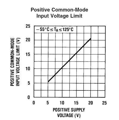
Note that the positive common-mode input voltage limit is always a little higher than the positive power supply rail voltage. True, it isn’t by much, but we only want to match this voltage, not exceed it. After a bit more digging, the following words of advice appear in the datasheet:
The second paragraph seems to give the green light and the last paragraph warns us not to use this OpAmp with only a 6.3V power supply differential, something that I was tempted to try. Of course, the LF412 is not the only OpAmp that could be used. In fact, it is ancient solid-state terms. Nonetheless, it is still in production, quite competent, and cheap. LF412 Specifications
If I were designing this no-gain line stage today (actually, I am thinking of using a variation on the circuit for a project I have in mind), I would look into CMOS-based OpAmps that can accept huge positive common-mode voltage input voltages. Ah, so many experiments and so little time. //JRB |
Only $12.95
Download or CD ROM www.glass-ware.com
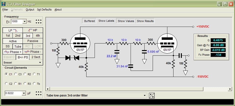
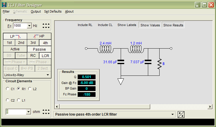
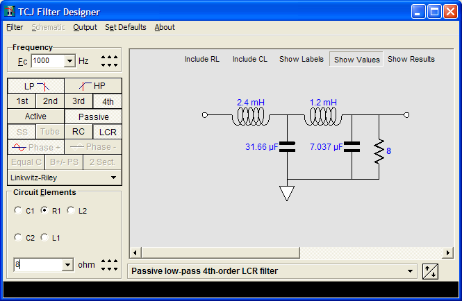
The Tube CAD Journal's first companion program, TCJ Filter Design lets you design a filter or crossover (passive, solid-state or tube) without having to check out thick textbooks from the library and without having to breakout the scientific calculator. This program's goal is to provide a quick and easy display not only of the frequency response, but also of the resistor and capacitor values for a passive and active filters and crossovers. TCJ Filter Design is easy to use, but not lightweight, holding over 60 different filter topologies and up to four filter alignments: While the program’s main concern is active filters, solid-state and tube, it also does passive filters. In fact, it can be used to calculate passive crossovers for use with speakers by entering 8 ohms as the terminating resistance. Click on the image below to see the full screen capture.
Tube crossovers are a major part of this program; both buffered and un-buffered tube based filters along with mono-polar and bipolar power supply topologies are covered. Available on a CD-ROM and a downloadable version (4 Megabytes). Download or CD ROM
|
|||
.png)


| www.tubecad.com Copyright © 1999-2007 GlassWare All Rights Reserved |