As can be seen, from the equivalent circuit, interface will allow high frequencies to go through with very little attenuation whereas the lower frequencies will be attenuated to a limit which is the amount of resistance in the resistive-capacitive network. In practice, where pulses are used for testing purposes, the leading edge of the pulse will show a "spike"
when applied to a tube with a bad degree of interface impedance and the trailing edge of the pulse will be at a lower level or plateau. Where sine wave frequencies are used for testing, the high frequency sine waves receive very little attenuation, whereas the lower frequency sine waves receive more attenuation, depending upon the amount of resistance in the interface impedance.
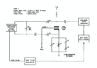
In the Frost System* of measurement, resistive and inductive components are placed in series with the cathode lead. Excitation is supplied by a squarewave generator, Figure 3. The complementary resistance and inductance network is varied until an output wave shape is obtained which is flat for all frequencies. This is combined with a gain measuring device to obtain complete attenuation of all pulse frequency components except the distortion which is produced by the interface impedance. By bucking the positive and negative going pulses on the oscilloscope, a balance is reached when a single straight line is obtained. The resulting resistive and inductive components in the cathode leads give the information necessary for computing interface capacities. The resistance inserted in the complementary network is essentially equal to the interface resistance.
Some tube types now have specification controls on interface resistance. Interface resistance measurements of a sample of tubes produce a random order of interface values which is widely dispersed; therefore, it is impossible to apply normal statistical techniques for calculating mean or standard deviations of interface values which have any degree of
certainty. In order to maintain the tubes within specification limits therefore, the interface resistance level of the bulk of the tubes in any sample must be maintained far below the specified limit. Interface resistance controls as presently established will allow only a very small number of tubes from a large life test sample to exceed the specified interface resistance level.
Since the compounds which cause the difficulties have been determined, the various tube manufacturers have attempted to control these elements in their tube components and processes. All present day emission coatings contain a fair percentage of barium and oxygen; therefore, the only element which can be controlled in the case of barium orthosilicate (Ba2SiO4) is the silicon. Present-day active cathodes seldom have silicon contents in excess of .03 907 and some critical tube types use cathode materials which have a silicon content of .01 % or less. The barium orthosilicate layers still form but their thickness and maximum impedance are limited by the available silicon within the volume of nickel alloy which makes up the cathode. Other cathode materials give good interface resistance effects which are due to elements which maintain the electrical activity of the barium orthosilicate layer.
|
Fig 3 Partial Diagram of Frost circuit for measuring interface impedance. (Click to see enlargement) |
||
|
|
||