|
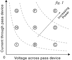
The dashed lines are contours of constant power, with device power dissipation increasing to the upper right corner.
For the pass device to work successfully, it must be linear and have gain at all the points on the graph. The two most difficult points are E and G. Point E is obviously difficult, since it is the point of maximum power dissipation. The reason point G is difficult is that it is hard for some active devices to pass a lot of current at low voltages.
Pentode-Type Pass Devices
Pentodes, beam-tetrodes, bipolar transistors, and MOSFETs all have constant-current characteristics, i.e. at a constant control voltage or current, the current passed through the device doesn't change much with voltage. Ideally, the characteristic curves for these devices would be horizontal lines. At low voltages, however, constant current cannot be maintained and the curves fold down toward zero.
Bipolar transistors and enhancement-mode MOSFETs have no hard upper limit to the current drawn, other than limited drive current or voltage, or maximum ratings. Bipolar transistors are especially good at low voltages, but have "second-breakdown" problems with simultaneous high current and high voltage. For them, point E is the hardest to maintain. MOSFETs are better in this regard, but still can be blown by transient high voltages or currents. For high-current regulators, the base current drawn by bipolar transistors becomes a problem. Power bipolar transistors can also have relatively slow speed, hurting high frequency response. MOSFETs have essentially infinite input resistance and inherently faster behavior, but their input capacitance is high and highly variable with operating point, making good high frequency response difficult.
Beam tetrodes and pentodes (which behave similarly) have very low input resistance and capacitance. Their behavior at low plate voltage is not as good as the solid-state devices, but their immunity to transient over-voltage and over-current is superb. One limitation, however, is the need to keep the grid negative with respect to the cathode. When the grid goes positive, grid current flows, causing difficulty to the grid drive circuit. Many receiving-type tubes are not designed for positive grid operation, so, even though it may work, reliability is not assured. The characteristic curve for Eg = 0 sets an upper limit for current. Fig. 2 shows the curves for a pentode that has enough current capability for the job. If a wimpy pentode or a pentode with insufficient screen voltage is used, as in fig. 3, then the high current situations at points E, F, and G won't be handled.
If a pentode with adequate current capability is available, why isn't it the perfect device for a regulator? One problem
|
|