shown in figure 4.3. Here the voltage divider and Vref are turned "upside-down". This topology is handy when a solid-state Op Amp and Vref are used in a high-voltage supply. These devices are run off of a floating supply connected to Vout and R1 "reaches" a long way down to ground.

Practical Implementations
Now let's look at how these regulator topologies can be used in actual designs. The emphasis here is on tube implementations, but semiconductor discrete devices can be used, too. The subtleties of compensating for semiconductor temperature drift will not be covered here.

Figure 4.5 shows a slight rearrangement of figure 4.4, where the ground connection is moved up to the plus input and the bottom of R2 now connects to a negative Vref. A single Vref can now supply many regulators.

   Figure 4.6 shows the most common implementation of a vacuum-tube series regulator. V1 is the pass tube, V2 is the comparison device and V3 is a gas regulator tube. As mentioned in the previous installment, V1 is typically a low-mu, high transconductance triode. V2 should be as high gain as possible, so its usually a high-mu triode, such as 1/2 or a 12AX7 or 1/2 of a 6SL7GT. V3 is typically a 75V or 105V regulator, like the 0A3, 0C2, 0C3, or 0B2. If the current through V2 is kept low, a reference tube such as the 5651 or 0G3/85A2 could be used. The values of R1, R2, and C1 are as described above. R4 is chosen so that the sum of the current through V2 and R4 puts the regulator into a stable operating region: about 2 mA for the 5651/0G3/85A2 and 10 to 15 mA for the larger regulators. Iv3 = Iv2 plus (Vout - Vref)/R4

Series Regulator where the plus input connected to the negative "power supply" connection of the device.

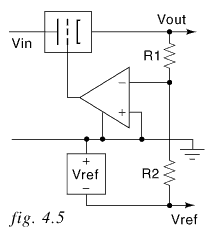
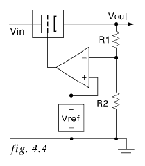
   The simplest comparison device is a single voltage-amplifying device, such as a tube, FET or transistor. The "minus" input is the grid, gate, or base, and the "plus" input is the cathode, source, or emitter. Since this "plus" input is also the negative device current connection, figure 4.2 was redraw in figure 4.4 to show the plus input connected to the negative "power supply" connection of the device.
   There is a significant offset voltage between the minus and plus inputs of a single-ended comparison device, ranging from 0.7 volts for a transistor to several volts for a tube or FET. This offset voltage is fairly constant, though, so we can compensate for it by slightly changing the R1 and R2 ratio, according to: Vout = (Vref plus Voffset) * ((R1 plus R2)/R2). Remember that for a tube, n-channel depletion mode FETs and PNP transistors, the offset voltage is negative.
   The circuit in figure 4.4 has the problem that the comparison device current runs through the voltage reference. Many voltage references are imperfect, and changes in current can lead to changes in Vref, reducing the quality of regulation. This circuit also requires a voltage reference for each regulator: a complication and expense when multiple regulators are used.

Series Regulator with a tube voltage reference 

< PREVIOUS

www.tubecad.com   Copyright © 1999 GlassWare   All Rights Reserved