|
|
MOSFETs, on the other hand, have a much softer transition from off to on, which requires the heftier idle current of a rich Class-AB operation, say 200 mA versus the 50 mA of a transistor output stage. In other words, setting the bias to the lowest distortion point is going to be much more important in a Class-AB buffer than a Class-A buffer.
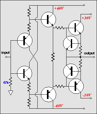
One possible buffer circuit is shown below. This buffer comprises only three current gain stages, so transistor selection is critical. Furthermore it requires two rail voltages, as the front-end circuit is not constant current source loaded. In addition, the buffer has a small insertion loss due to the voltage divider at each input transistor's emitter, which allows the output transistors to be properly biased.
|
|
|
|
Global Feedback Buffers
This type of buffer is actually just a conventional feedback amplifier with all of the gain being returned to the input stage. So can any power amplifier be turned into a global feedback buffer? No, as not all power amplifiers are unity gain stable for starters. Second, the average amplifier was designed under the assumption that the input voltage would not exceed a few volts and that, as a result, the input stage's voltage relationships would remain pretty much fixed. The current sources, the collector resistors, and the cascoding circuitry --all would see a fairly stable, fixed voltage. But when the input voltage must equal the output voltage, the whole of input stage must follow along the large voltage swings. (Here is where examining Op-Amp circuits is valuable, as Op-Amp must work in spite of huge input voltage swings. In sum, a power buffer needs to be designed from the ground up.)
Current Feedback
One circuit topology that causes much confusion is the current-feedback amplifier, marked by high speed and wide bandwidth; it achieves these results by breaking away from the normal Op-Amp ideal of ultra-high input impedance and zero input current at each of its inputs. In contrast, the current feedback amplifier has an ultra-low input impedance and zero input voltage (at least at its negative input). Returning the feedback to the input stage's emitter, rather than its base, realizes this goal and it ensures that the internal capacitances do not limit the Op-Amp's performance. The price paid for this benefit is the cost of having to drive the low impedance feedback pin. But in a power buffer application, this proves easy, as the output's output will easily drive input stage's emitters. So what is needed to make a current-feedback power buffer? First of all, we cannot use a conventional differential input stage, as its negative input is of the high impedance sort. Instead, we must try to drive emitters of the input stage as a negative feedback entry point.
|
|